Technologists from DNP and Nikon Discuss Computational Lithography Solutions
Earlier this year, Naoya Hayashi, Dai Nippon Printing Company Fellow, delivered a presentation at the LithoVision technical symposium entitled “Computational Lithography Requirements and Challenges for Mask Making”. Hayashi began his informative talk by showing the 2011 ITRS Roadmap, and noting that optical lithography extension is expected. He explained that there are a number of advanced computational lithography options, including more complex optical proximity correction (OPC), source mask optimization (SMO), and inverse lithography technology (ILT). He stressed that using solutions such as SMO is imperative.
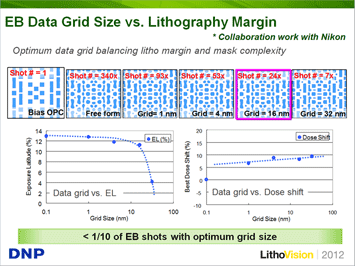
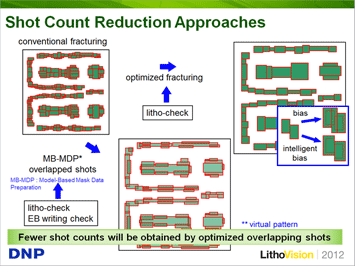
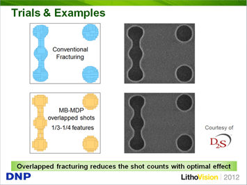
Hayashi reported that as a result of all of these techniques, mask data is becoming more complex and intensive. He started with work optimizing the ebeam (EB) data grid size in order to balance the litho process margin and the mask complexity to maintain manufacturability. He described various mask shot count reduction approaches, noting that fewer shot counts will be obtained by optimizing overlapping shots using model-based mask data preparation (MB-MDP) and by using dedicated shot shapes. He also shared trial results (courtesy of D2S, Inc.) confirming that overlapped fracturing successfully reduced the shot counts to 1/3-1/4 of the conventional fracturing features and delivered the best results.
-
Click image to enlarge.
Click image to enlarge.

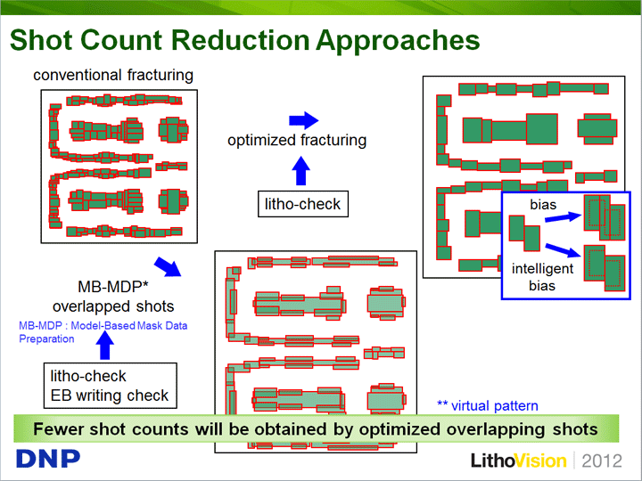
Figure 1. Hayashi described work optimizing the EB data grid size in order to balance the litho process margin and mask complexity (left image). He also reported that fewer shot counts will be obtained by optimizing overlapping shots using MB-MDP preparation.
Hayashi reported that mask defect inspection and printability metrology tools for computational lithography masks have been evaluated as well. Advanced mask defect inspection tools with capabilities to 22 nm and pixel sizes on the order of 50-70 nm, such as those offered by KLA-Tencor and NuFlare Technology Inc., are essential. He also commented that printability metrology tools having 22 nm capabilities, excellent accuracy and repeatability, and SMO applicability will be needed as well.
In Hayashi’s closing remarks he reminded the audience that while ArF will be extended with computational litho, the mask data is becoming more complex and intensive. He concluded that successful trials are underway to reduce shot counts, and noted that continued collaboration among mask suppliers and users as well as other related tool suppliers is necessary.
-
Click image to enlarge.
Click image to enlarge.
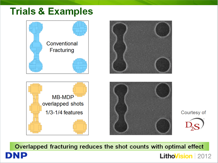
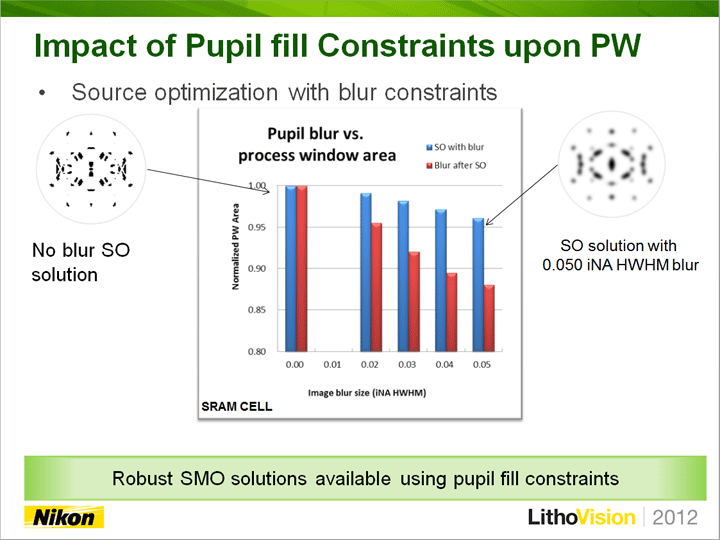
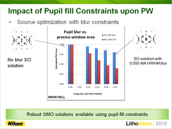
Figure 2. Hayashi shared trial results that confirmed overlapped fracturing reduced the shot counts significantly and delivered the best results (left image). Matsuyama highlighted that robust SMO solutions taking constraints into consideration are available.
The next speaker at LithoVision, Tomoyuki Matsuyama, Nikon Strategic Imaging Solutions Section Manager, delivered a presentation addressing computational lithography from the scanner perspective. He showed that the key scanner elements in the computational litho value chain include pupilgram setting, optical proximity error (OPE) optimization, thermal aberration setting, and exposure capabilities, and stressed that systematic and automatic procedures are required.
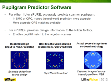
Matsuyama first explained that exotic pupil fills are required for SMO and noted that custom s-PURE elements can be made to create any pattern, with the resulting pupilgrams having zoom and annular-ratio adjustment capabilities. He then reported that the Nikon Intelligent Illuminator unit (IIU) provides complete adjustability, providing both parametric pupil fills and free-form pupil fills. Matsuyama noted that pupil blur size and pupil fill ratio constrain the process window and said that robust SMO solutions that take these constraints into consideration are available. Matsuyama next discussed the criticality of pupilgram prediction and reported that the Nikon Pupilgram Predictor closely predicts a scanner pupilgram from either s-PURE elements or the IIU. He explained that this will make the SMO and OPC predictions more accurate, thereby enabling enhanced OPE matching capabilities and illuminator pupilgram design.
-
Click image to enlarge.
Click image to enlarge.
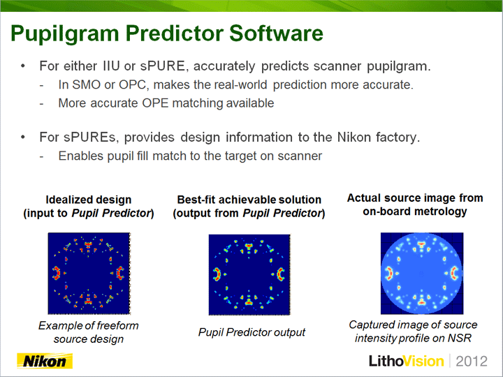
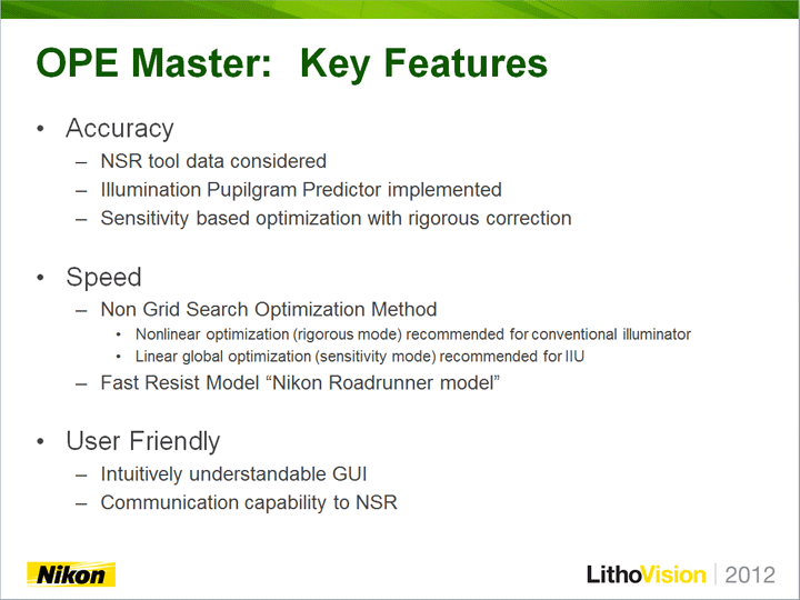
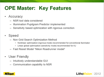
Figure 3. Matsuyama reported that the Nikon Pupilgram Predictor closely predicts a scanner pupilgram from either s-PURE elements or the IIU (left image). Matsuyama reported the key features and benefits of OPE Master.
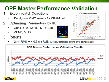
Matsuyama also described a solution for tuning OPE performance that takes advantage of the Intelligent Illuminator degrees of freedom. He reported that Nikon OPE Master application software enables OPE matching using a high degree of pupilgram modulation freedom, and highlighted this solution’s accuracy, speed, and user-friendly capabilities. Matsuyama noted that a vital component of this software is the use of actual NSR tool data. OPE Master retrieves tool-to-match imaging-related data for more accurate modeling and then sends the optimization results back to the scanner automatically. He further explained that OPE Master can optimize pupilgram modulations generated by the IIU that include Zernike distortion modulation, Zernike intensity modulation, pupil blur size, and background flare. Matsuyama shared OPE Master validation results showing RMS data reduced from 2.0 nm to < 0.7 nm using SMO pupilgram results for an SRAM cell, and optimizing various Zernike-type patterns in the Intelligent Illuminator unit.
-
Click image to enlarge.
Click image to enlarge.

Figure 4. OPE Master validation results showed RMS data reduced from 2.0 nm to < 0.7 nm (left image). Matsuyama reminded the audience that fast and accurate setting of the scanner is essential to the success of computational lithography.
In the final section of his presentation, Matsuyama cautioned the audience that these exotic pupil fills generate higher thermal aberrations, and stated that a quick method for thermal aberration prediction and control is needed to make SMO solutions viable on scanners. He reported that the Thermal Aberration Optimizer (ThAO) successfully predicts and optimizes thermal behavior on the scanner, and does so free of time-consuming lens heat tests. Matsuyama described how during the lot, the Intelligent Lens Controller (LC) measures thermal aberrations such as focus, curvature, magnification, distortion and wavefront aberrations every few wafers. He explained how thermal calibration is performed and that the scanner parameters are fine-tuned based on the measurement results, with the tuned parameters then used for the second and subsequent lots.
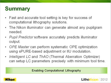
Matsuyama concluded by reminding the audience that fast and accurate setting of the scanner is essential to the success of computational lithography. He emphasized that the Nikon IIU, Pupil Predictor, OPE Master, Intelligent Lens Controller, and ThAO are innovative solutions that satisfy these critical requirements for IC makers.