The Future of 450 mm and EUV Highlighted at LithoVision
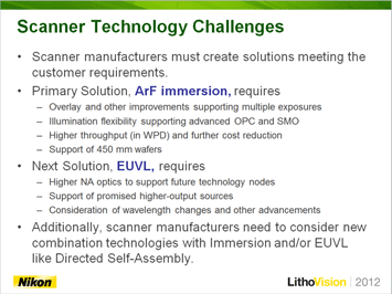
In his presentation addressing the Nikon view of the Lithography Roadmap and Future Devices, Masato Hamatani, General Manager of Stepper Development, reported that ArF immersion is the primary lithography solution to satisfy customer requirements and noted that it is able to support sub-20 nm half pitch (hp) processes. However, he cautioned that in addition to enabling multiple exposures, supporting advanced optical proximity correction (OPC) and source mask optimization (SMO), and providing higher throughput— ArF immersion extension also requires support of 450 mm wafers.
-
Click image to enlarge.
Click image to enlarge.
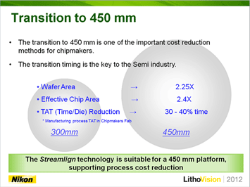
Figure 1. Hamatani reported that ArF immersion is the primary lithography solution (left image). He explained that the transition to 450 mm is one of the most important cost reduction methods for chip makers.
Hamatani reported that the transition to 450 mm wafers is one of the most important cost reduction methods for chip makers, with wafer area increasing by 2.25x and effective chip area rising by 2.4x. However, he cautioned that the transition timing is imperative to the semiconductor industry. Hamatani announced that Streamlign technology, like that already employed on NSR-S62X and S320F systems, is suitable for a 450 mm platform to support this critical process cost reduction. He then explained that the “next” potential lithography solution, EUVL, will require increased optics’ numerical apertures (NA), compatibility with higher-output sources (when they’re available), as well as consideration of changes in exposure wavelength and/other advancements. Hamatani stated that Nikon is pursuing advances in EUV optics, including high-NA designs and reduced flare, to be ready when the industry infrastructure has matured.
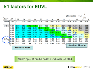
Later in the symposium, Katsuhiko Murakami, Nikon EUVL Team Leader, discussed the latest technical challenges of EUV lithography. He reported that the currently available power source is below 10 watts, while more than 100 watts are actually required. Murakami also highlighted that while defect-free mask blanks are necessary, defect density still needs to be reduced by approximately 100x. He explained that this challenge is further compounded by a lack of sufficient mask inspection tool capability. Murakami also noted that that resist resolution, linewidth roughness (LWR), and sensitivity need continued improvements, and optics contamination due to resist outgassing must also be addressed. In light of the magnitude of these challenges, Murakami reported that Nikon believes the current infrastructure challenges make EUVL non-viable for insertion into high volume manufacturing at this time. Murakami proceeded to explain that an NA of 0.25 will only support resolution of 18-16 nm, while an NA of 0.33 to 0.35 could be used for the 16 nm half-pitch (hp). However, at the 11 nm node, such an NA would correspond to a k1 factor less than 0.3, which is approaching theoretical limits and is very difficult to achieve. Therefore, he commented that an NA value greater than 0.4 will be needed to enable multi-generational use for 16-11 nm hp nodes and avoid the need to do Double Patterning with EUVL. Murakami reported that Nikon is preparing NA > 0.4 lens designs to make EUVL ready for future nodes, while continuing efforts in lens aberration reduction.
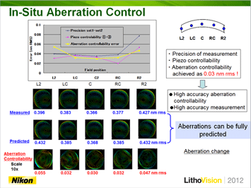
Murakami also highlighted that tool stability with regard to optics and mask contamination, the source, and in-situ optimization are key factors in high volume manufacturing. He commented that progress has been made in these areas. Murakami reported that a comprehensive strategy to mitigate carbon contamination, surface oxidation, and other silicon containing compounds has been established. He further shared that Nikon has successfully developed and demonstrated an in-situ aberration control system using a multi-incoherent source Talbot interferometer (MISTI) on the EUV1 system. He described this as a type of shearing interferometer that measures the wavefront of the projection optics on-body. Murakami showed that with the MISTI interferometer, Nikon can set optical aberrations to within 0.03 nm RMS of a target, and noted that this high level of controllability would be applied to HVM EUV tools.
-
Click image to enlarge.
Click image to enlarge.

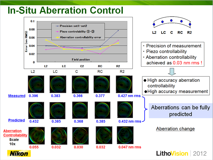
Figure 2. Murakami reported that NA >0.4 will be needed to to enable multi-generational use for 16-11 nm hp nodes (left image). He showed that with the MISTI interferometer, Nikon can set optical aberrations to within 0.03 nm RMS of a target.
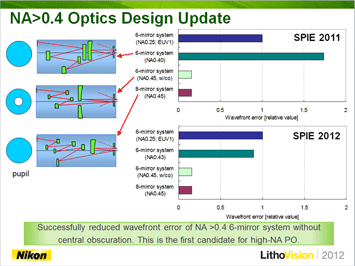
Speaking in more detail about enabling higher resolution, Murakami explained that Nikon has been investigating several different types of projection optics designs, focusing efforts on improving the optical design of a conventional 6-mirror system. He reported that Nikon successfully reduced the wavefront error of a 6-mirror system having a numerical aperture >0.4 to the same level as the 0.25 NA EUV1 optics. This was achieved in a design without a central obscuration, which can cause problems with forbidden-pitch patterns in small sigma illumination. This six-mirror design without central obscuration is the first candidate for the Nikon high-NA projection optics design.
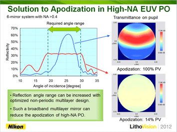
Murakami said that high-NA optics require a larger angle of reflection than 0.25 NA optics, but cautioned that conventional multi-layer mirrors have a periodic structure which provides an insufficient reflection angle range, and thereby causes strong non-uniformity of pupil transmittance, called apodization. Murakami explained that the solution for this is use of broadband multi-layer coatings that have non-periodic structures, and he shared data demonstrating how non-uniformity was reduced to only 14% using the broadband multi-layer coatings. Murakami reported that these broadband multi-layer mirrors have been developed and that the measured reflectivity profile agreed very well with the designed profile, confirming that the apodization issue can be mitigated using broadband multi-layer mirrors.
-
Click image to enlarge.
Click image to enlarge.


Figure 3. Murakami reported that Nikon has successfully reduced the wavefront error of a 6-mirror system having a numerical aperture >0.4, without central obscuration (left image). Non-uniformity was reduced to only 14% using broadband multi-layer coatings.
Murakami summarized his detailed presentation by reminding the audience that due to infrastructure challenges, Nikon believes that the realistic EUVL high volume manufacturing insertion will be for 16-11 nm nodes. He reiterated that Nikon is actively continuing EUVL development and concluded high volume manufacturing performance requirements have been achieved in the areas of projection optics NA >0.4, multi-layer coatings improvement, and contamination control.