Extending ArFi to 22 nm and Beyond with Advanced CDU Control
At the recent SPIE Advanced Lithography conference, Nikon System Engineer, Tomoharu Fujiwara, reported that CD uniformity (CDU) for 2x nm nodes must be improved from present levels. He explained that ArF immersion (ArFi) is expected to be utilized with various double patterning (DP) schemes for these nodes and beyond. He then described how for spacer DP, CDU requirements are actually split into two parts – core gap CD control and line deposited sidewall thickness uniformity. Fujiwara proceeded to explain that according to the 2010 ITRS roadmap, the core gap CD control requirement is 1.1 nm 3σ for the 20 nm technology node. He cautioned the audience that to achieve this CDU with sufficient margins, particularly in the case of high volume manufacturing (HVM), sophisticated scanner dose and focus adjustments able to compensate for process errors are vital.
Fujiwara reported that Nikon has been actively developing solutions to address the aggressive 2x nm node requirements, and introduced the CDU Master product, a software application designed to enhance CD uniformity for patterns imaged on Nikon scanners. He went on to describe the CDU Master operation flow. The system calibrates through-focus and through-dose CD behavior through a one-time measurement of a focus-exposure monitor (FEM) wafer. Then, a standard wafer is exposed on the Nikon scanner and CD measurements are taken, typically by a CD-SEM or scatterometry tool. The software then analyzes the CD uniformity errors and calculates custom focus and dose adjustments to minimize CD variation, regardless of their source. This includes compensation for variation in the resist thickness, post exposure bake (PEB) temperature, wafer flatness, reticle components, etc. These error factors all have a significant influence on CDU, but are relatively stable and can be corrected for via precise dose and focus adjustment functions on the scanner. CDU Master then generates a sub-recipe, which includes high order focus and dose correction values for each exposure field, that is subsequently used by the NSR during wafer processing. Fujiwara noted that these values are calculated in accordance with tool-specific tolerances and limits.
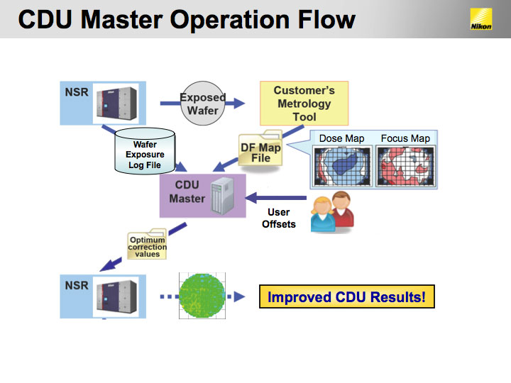
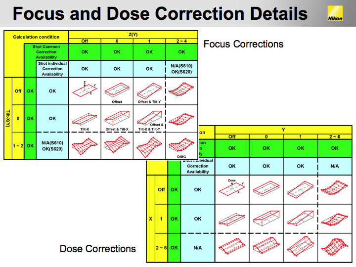
Figure 1. CDU Master operation flow (left image). Sophisticated focus and dose corrections on the scanner are used to compensate for process-related CDU errors.
Focusing on the specifics of CDU Master capabilities, Fujiwara explained the intra-field dose correction functions. He described that up to 6
Fujiwara then demonstrated results obtained with CDU Master. He began by showing NSR-S620D CD data collected from the KLA-Tencor SCD100, with dose and focus maps calculated using the KLA-Tencor KT-Analyzer software. In this case, the calculated correction values were 3% for dose and 50 nm for focus. Fujiwara highlighted that after CDU Master removed the correctable field-common components, CD variation was significantly reduced. He noted a small amount of 1
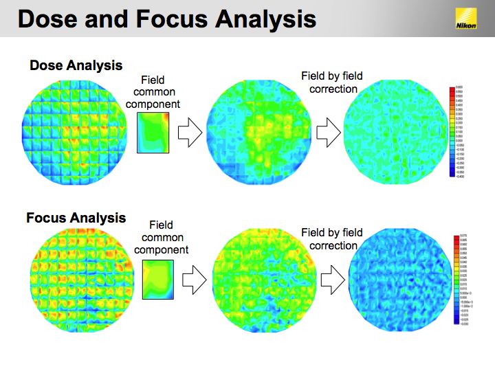
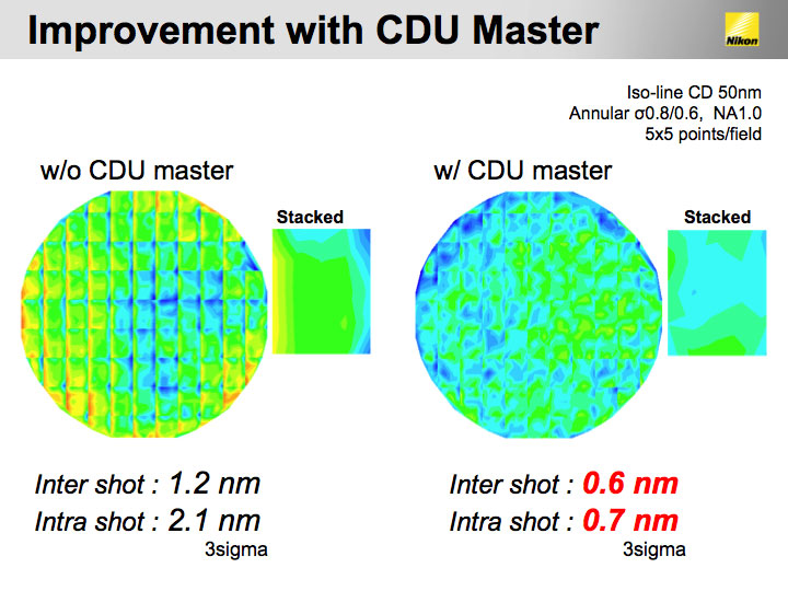
Figure 2. CDU Master corrects for field-common and field-by-field components (left image). CDU Master has reduced intrashot CD errors by more than 60%, and cut intershot errors in half.
Fujiwara also showed CDU Master results from another example, this time using an actual logic device gate on a shallow trench isolation (STI) layer. He noted that in this scenario, the CD measurement and correction was done using CD-SEM data with an analysis method recently developed by Hitachi High-Technologies. (View the LithoVision poster on this technique.) All structures showed significant improvements in CD uniformity using the CDU Master adjustments, this being a reduction of 40% in CDU for both interfield and intrafield results for isolated lines, and between 10 and 25% for dense features.
CD Improvement for Device Gate
| Measured by: CD-SEM CG4000 |
Before CDU Master Adjustment | After CDU Master Adjustment | ||
|---|---|---|---|---|
| iso | dense | iso | dense | |
| Inter field (nm, 3σ) | 1.1 | 0.8 | 0.7 | 0.7 |
| Intra field (nm, 3σ) | 1.1 | 1.6 | 0.7 | 1.2 |
Data courtesy of Hitachi High-Technologies
Concluding his presentation, Fujiwara stressed that field-by-field, high order dose and focus scanner correction capabilities to compensate for process errors are required for 2x nm applications and beyond. He showed that CD uniformity below 1 nm (intershot and intrashot) has been obtained using CDU Master; and also highlighted CDU Master flexibility, noting that it is compatible with scatterometry, CD-SEM, and AMI metrology systems.