Advanced Binary Film for 193 nm Lithography Extension to Sub-32 nm Node
As ArF lithography is extended, mask fabrication costs are becoming a bigger part of the IC manufacturing budget, especially with the adoption of double patterning (DP) techniques. ArF extension requires advanced optical proximity correction (OPC) methods that boost mask complexity and manufacturing costs. As added challenges, ArF reticles are also susceptible to haze, CD growth, and changes in the films themselves that will reduce mask lifetime, while larger mask error enhancement factors (MEEF) and stringent design rules make CDU specifications tighter. This in turn shrinks the tolerance for CD changes after mask cleaning/pellicle replacement, which decreases the permissible cleaning frequency. To alleviate this multitude of mask manufacturing, cost, and maintenance challenges, Hoya Corporation has developed a new Advanced Binary Film (ABF) to provide improved durability against cleaning and ArF irradiation effects.
After we investigated e-beam tool compatibility, dry-etching characteristics and mask cleaning durability, we selected tantalum (Ta), chromium (Cr), and silicon (Si) as candidates for the new mask absorber film. Cr however, was eliminated due to evidence of deposits being produced after ArF irradiation. Si was also judged unacceptable as it exhibited a transformation layer that increased in thickness when exposed to the 30 kJ/cm
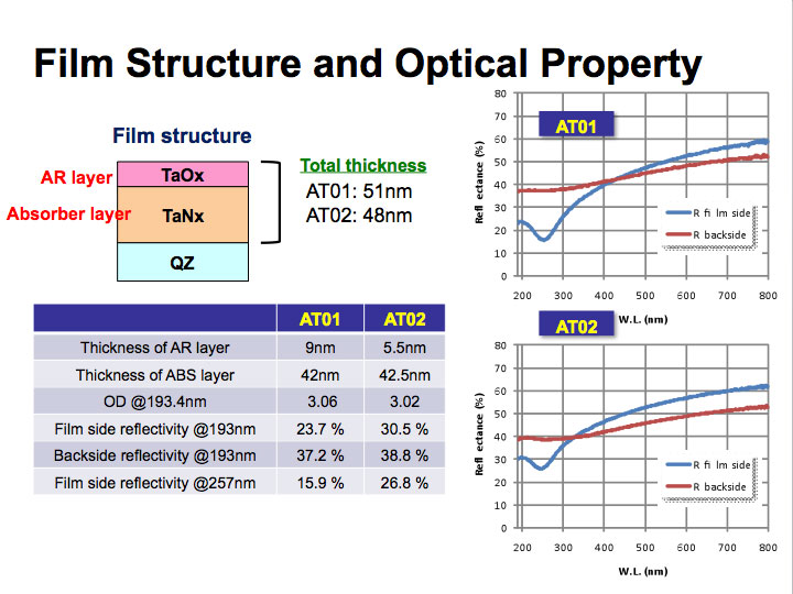
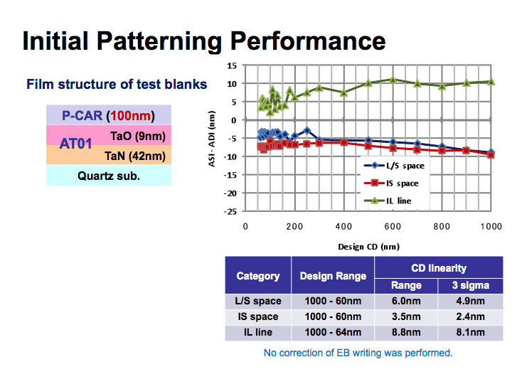
Figure 1. A thin film is achieved with sufficient optical density (>3.0) and optimized reflectivity (left image). AT01 can be patterned using 100 nm thick resist, with acceptable CD linearity demonstrated across various patterns.
We then looked at the patterning performance by coating 100 nm of positive-tone chemically-amplified resist on the ABF material, exposing it with a 50 keV electron beam tool, and evaluating the patterned images. Cross sectional SEM images confirmed vertical profiles were obtained for 60 nm line/space patterns, and line edge roughness of 3.5 nm (3σ) was demonstrated. CD linearity for various patterns was evaluated and AT01 was judged fully capable of patterning using 100 nm resist thickness.
Flatness change in the mask as a result of AT01 deposition was also studied as an indicator of film stress. The changes in total indicated range (TIR) flatness between the substrate alone and the blanks after the AT01 absorber film deposition were only -3, -12, and 14 nm, respectively, across the 3 plates evaluated, confirming that low stress is experienced with AT01. We also checked image placement error before and after the film process steps, and found that magnification change was near zero (-0.1 ~0 ppm). This high degree of performance will support customer efforts in dealing with the aggressive focus and overlay budgets required for advanced imaging processes.
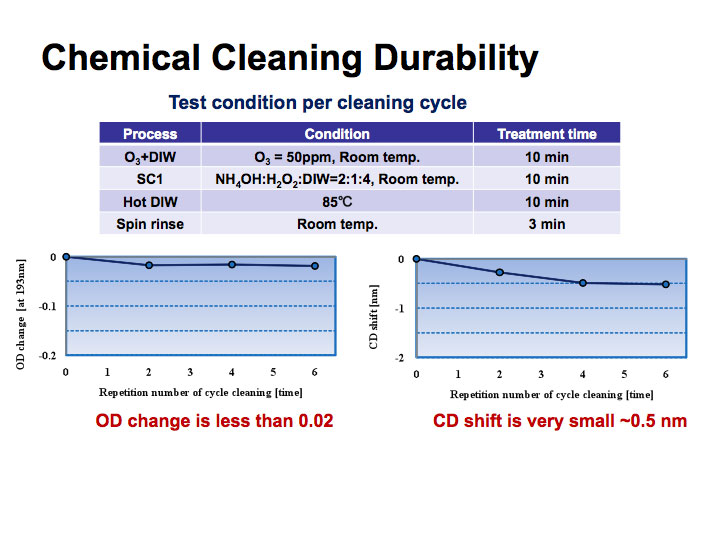
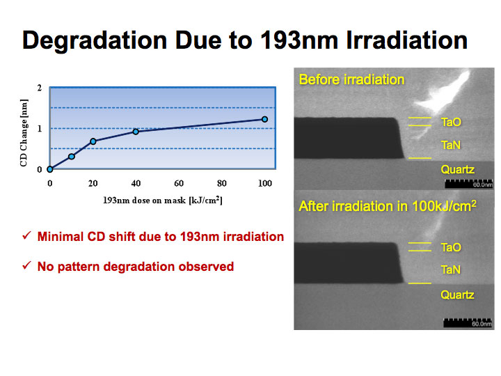
Figure 2. AT01 demonstrates excellent mask cleaning durability with very low OD change or CD shift (left image). Minimal CD shift (< 1.5 nm) and no pattern degradation due to 193 nm irradiation were also confirmed.
After these various qualification steps, it was necessary to investigate the new film’s durability to cleaning and ArF irradiation to see how well the ultimate development objectives were achieved. After six cycles of chemical cleaning, simulating cleaning during pellicle remounting, the optical density (OD) change was less than 0.02 (at 193 nm), and the CD shift observed was less than 0.5 nm. These changes are well within target specifications. Physical durability was verified with no pattern collapse experienced on 62 nm patterns. We also checked 193 nm irradiation effects by subjecting the patterned ABF mask with 200 nm L/S to a total ArF irradiation energy of 100 kJ/cm
ArF immersion lithography will be extended beyond the 32 nm node, and controlling mask performance and costs to satisfy aggressive double patterning requirements is vital. Hoya Corporation has developed two new advanced tantalum-based films to achieve this objective and AT01 has already successfully demonstrated high durability to mask cleaning and ArF irradiation. Both films are expected to significantly increase mask lifetimes for long-term savings in total mask costs for lithography.
View the LithoVision poster on this technology for more details.
Reference
[1] Nozawa et al., "Advanced Binary Film for 193 nm Lithography Extension to Sub-32 nm Node". Proceedings of SPIE Photomask Technology Vol. 7832, 78230K (2010).
Osamu Nozawa
Senior Staff Engineer
Hoya Corporation
Osamu_Nozawa@sngw.els.hoya.co.jp