LithoVision and SPIE Presentations Focus on Enabling 32 nm Production
At the recent LithoVision 2010 symposium,Yuichi Shibazaki, Nikon Next-Generation Product Manager and NSR-S620 Technical Director, provided an overview of the development and status of the Nikon lithography solution to enable 32 nm production. Shibazaki reported that Nikon development of the Streamlign platform actually began five years ago, and focused on satisfying the vital customer requirements of maximum yield, affordable lithography, and shortest time to profitability for IC makers.
To deliver on these requirements, Nikon targeted 2 nm overlay, 200 wafers per hour throughput, and 20 day installation for the Streamlign platform design. At LithoVision, Shibazaki reported significant achievements toward these program objectives, and announced that Nikon has been shipping the NSR-S620D ultra-high productivity immersion scanner for double patterning and 32 nm applications since Q4'2009. Using the Streamlign platform design, the NSR-S620D targets 200 wafers per hour throughput with a single exposure stage, and adopts a sophisticated hybrid control system to enable 2 nm overlay accuracy. The S620D also incorporates the recently developed Modular
Shibazaki shared S620D data demonstrating throughput >170 wafers per hour (WPH) in December 2009, fully on track to achieve 200 WPH by mid-2010 following changes to software, pneumatics, and amplifiers. The ultra-high throughput of the S620D is made possible by increased scan speed and improved acceleration capabilities to minimize exposure time, coupled with the newly developed Stream Alignment wafer mapping system that performs wafer alignment and focus mapping during wafer exchange to reduce overhead time. S620D reliability has also been thoroughly demonstrated with 24 hour wafer cycling executed free of any tool errors or interrupts. In addition, very low defectivity levels have been achieved at 700 mm/sec, which confirms the production-worthiness of the tool even at maximum scan speed.
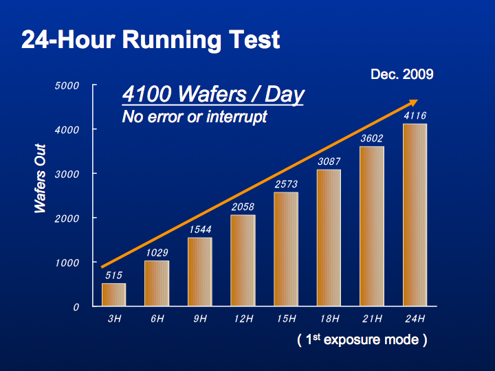
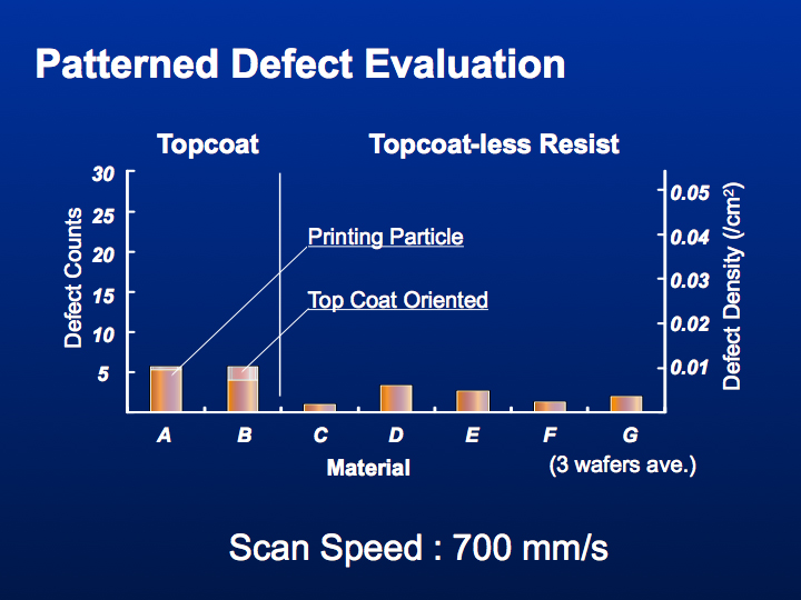
Figure 1. Shibazaki reported that S620D reliability has been thoroughly demonstrated with 24 hour wafer cycling executed free of any tool errors or interrupts (left image). In addition, very low defectivity has been achieved at 700 mm/sec, which confirms the production-worthiness of the tool even at maximum scan speed.
Shibazaki also provided an update on S620D accuracy performance. He showed repeatability improvements ≥ 50% for both stage accuracy and wafer autofocus mapping as a result of using stage encoders, as compared to traditional interferometers. He explained that the S620D Bird's Eye Control design actually uses laser encoders in conjunction with the interferometers, and stressed that this combination is essential for ideal performance with immersion lithography where the encoders could be "blinded" by a water droplet.
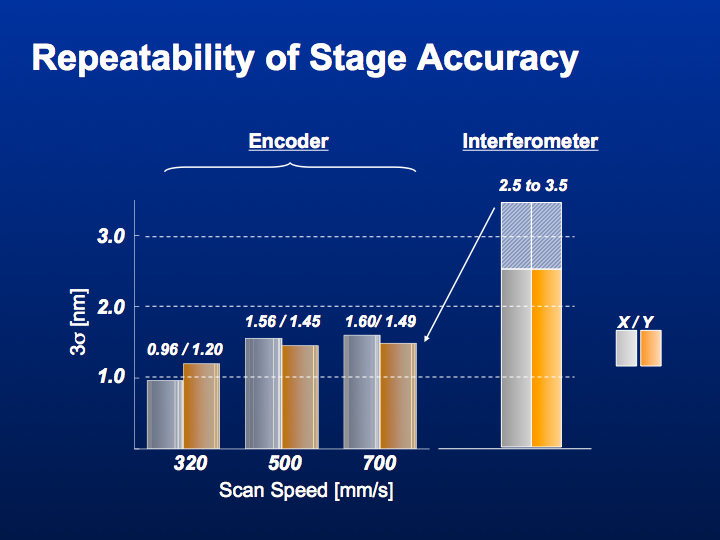
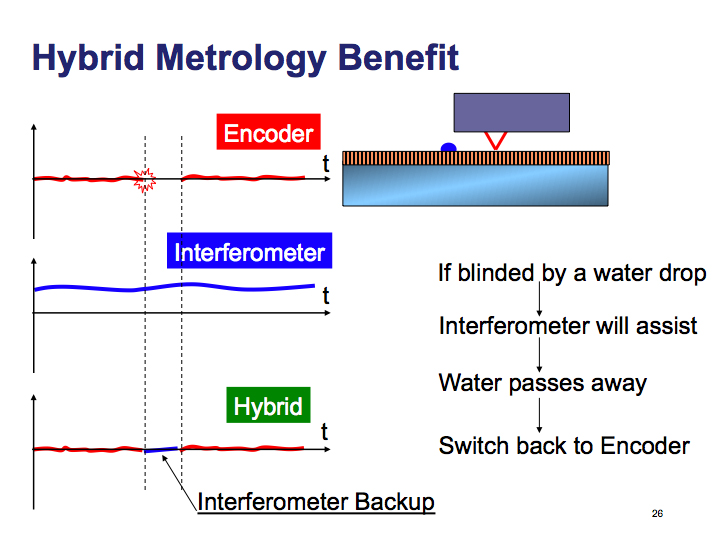
Figure 2. Stage accuracy repeatability was improved by ≥ 50% as a result of using stage encoders, as compared to traditional interferometers (left image). The S620D Bird's Eye Control uses laser encoders in conjunction with the interferometers to achieve ideal performance with immersion lithography where encoders could be "blinded" by a water droplet.
Speaking at SPIE Advanced Lithography later in the week Shinji Wakamoto, Manager of 2
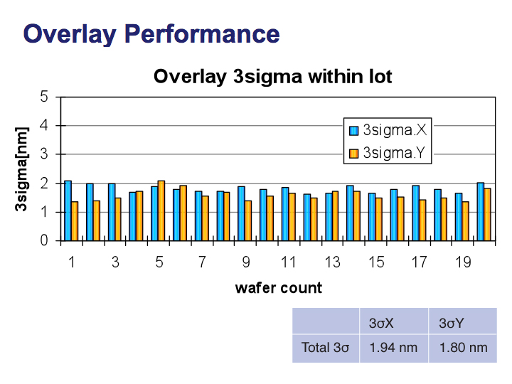
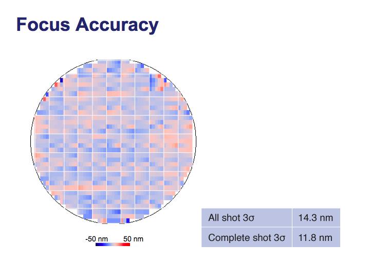
Figure 3. The S620D has demonstrated excellent accuracy and stability, and showed across-lot overlay 3σ data below 2 nm (left image), as well as across wafer focus control below 15 nm (3σ) for all shots.
Wakamoto continued with discussion of the S620D body design. He stressed the importance of CD control for 32 nm applications and beyond, and highlighted that structural vibration and stage synchronization error can both degrade CD uniformity. Therefore, to minimize these effects, the S620D uses the Modular
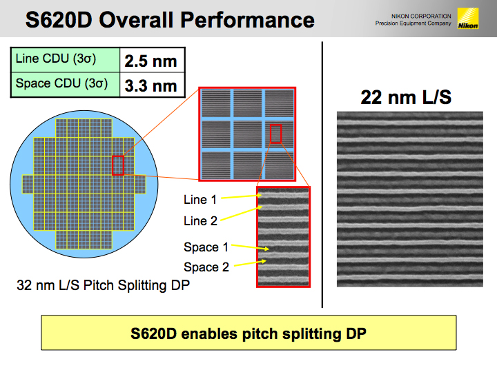
Figure 4. The S620D has demonstrated successful 32 nm pitch splitting across the entire wafer, as well as 22 nm capabilities.
In his final comments, Wakamoto summarized that with overlay accuracy < 2 nm, coupled with optimal focus and CD control, the S620D satisfies the aggressive requirements of the 32 nm half-pitch node and beyond. He then concluded his presentation showing S620D 32 nm pitch splitting double patterning results with features successfully resolved across the entire wafer, as well as 22 nm capabilities.