Samsung and Nikon Experts Report on Lithography Technology and Future Trends
Presenting his view on the Memory Roadmap and Challenges at the 2010 LithoVision symposium earlier this year, Dr. Jeong-Ho Yeo, Principal Engineer at Samsung Electronics reported that memory device scaling will be continued with a combination of double patterning technology (DPT) and EUVL. Dr. Yeo stressed that low cost DPT solutions such as litho-freeze-litho-etch (LELE), negative tone develop, and block copolymer methods will be vital in cost reduction for memory devices. He also noted that although DP overlay can be achieved with the latest scanners or with the use of self-aligned double patterning (SADP), further technology breakthroughs will be needed to achieve the stringent CD uniformity (CDU) requirements.
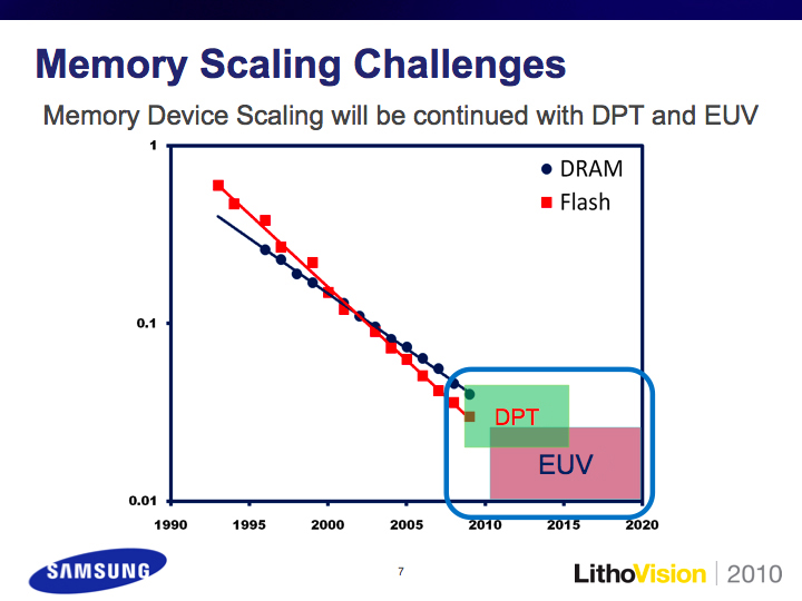
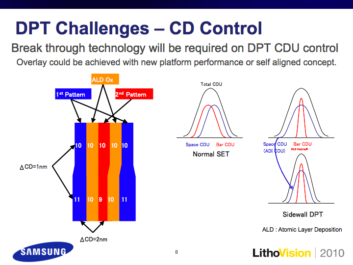
Figure 1. Dr. Yeo reported that memory device scaling will be continued with a combination of DPT and EUVL (left image). He highlighted that further technology breakthroughs will be needed to achieve the stringent DP CDU requirements.
Reporting on the state of EUVL, Dr. Yeo showed that resolution below 20 nm has already been demonstrated, and commented that industry EUVL readiness is continually improving. He noted that solutions should be achievable for the top three challenges, which include defect-free masks, source power, and resists for beyond 22 nm. When comparing EUV and DPT for near-term scaling, Dr. Yeo reported that EUV still has significant technical and timing challenges, whereas DPT struggles with cost of ownership (CoO) and extendibility. In his summary of the scaling success criteria for memory devices, Dr. Yeo identified cost reduction as the key parameter for DPT extension, and commented that below the 20 nm half pitch (hp), EUV may be the only lithography solution.
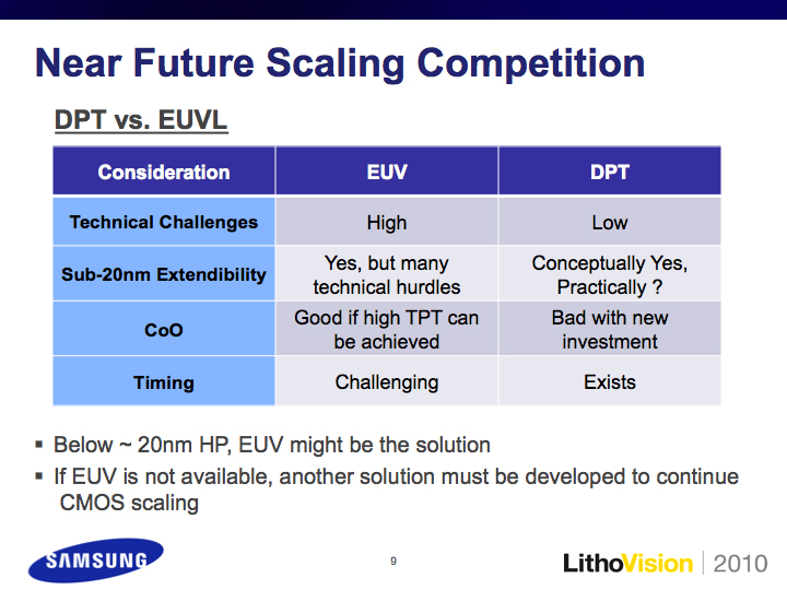
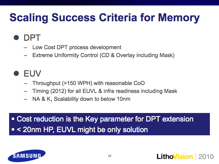
Figure 2. Dr. Yeo reported that EUV still has significant technical and timing challenges, whereas DPT struggles with CoO and extendibility (left image). He identified cost reduction as the key parameter for DPT extension, and commented that for < 20 nm hp, EUV may be the only solution.
In a complementary presentation, Masato Hamatani, GM of Nikon Stepper Development agreed that progress is being made with the EUV infrastructure. However, he noted that mask defectivity levels still dramatically exceed requirements and that critical inspection tools are not yet available. Given the timing associated with defect reduction efforts once the inspection tools are ready, Hamatani reported that EUV will likely not be a viable solution until around 2014, and stressed that this date is too late for many 22 nm roadmaps. He also noted that in large lot (many wafers/mask) scenarios EUVL cost of ownership is "just competitive" with double patterning, and highlighted that in order to enable multi-generational EUV tool usage, a lens numerical aperture > 0.35 will actually be required. Considering these various factors, Hamatani concluded that DP should be extended to 22 nm, with EUV implementation at 16 nm and beyond.
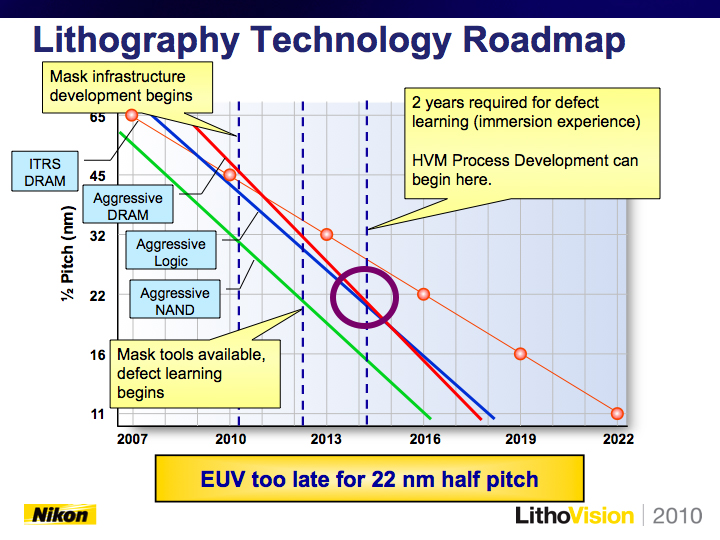
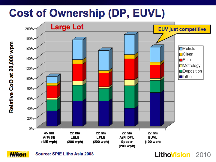
Figure 3. Hamatani commented that EUV will likely not be a viable solution until around 2014, and stressed that is too late for many 22 nm roadmaps (left image). He also noted that in large lot (many wafers/mask) scenarios EUVL cost of ownership is "just competitive" with double patterning.
Hamatani proceeded to discuss alternative solutions to EUVL using ArF immersion extension techniques such as spacer DP, pitch-splitting DP (LELE, litho-freeze-litho-etch, etc.), and line-cutting lithography. He then provided an update on the NSR-S620D immersion scanner for double patterning, and 32 nm applications and beyond. He reported that Nikon is shipping the ultra-high productivity NSR-S620D immersion scanner to meet the aggressive performance requirements for double patterning, and 32 nm applications and beyond. Hamatani summarized his presentation reiterating the obstacles of EUVL, and stressed the criticality of extending immersion double patterning using existing scanner platforms. In his closing, Hamatani stated that Nikon recognized these challenges for customers, and designed the S620D Streamlign Platform for extendibility to 22 nm applications and perhaps further.