LithoVision Expert Panel: 10 Years of Litho – A Review and Look Ahead
At the 10th annual LithoVision event, technology leaders from AZ Electronic Materials, Intel, Dai Nippon Printing, Fraunhofer IISB, Synopsys and Nikon shared their opinions regarding key lithography events and innovations of the past 10 years, and discussed potential “game changers” for the future during an interactive panel session moderated by Dr. Donis Flagello of Nikon Research Corporation of America. Participating in the panel were Naoya Hayashi, Fellow at Dai Nippon Printing (DNP); Dr. Ralph Dammel, CTO of AZ Electronic Materials; Dr. Kevin Lucas, OPC and RET Product Engineering Manager for Synopsys; Dr. Andreas Erdmann, head of the Lithography Simulation Group at Fraunhofer IISB; Sam Sivakumar, Intel Corporation Fellow and Director of Lithography; and Dr. Soichi Owa, Nikon Fellow.
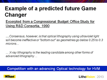
Dr. Flagello opened the panel session by identifying a past key game changer─ the chemical mechanical polish (CMP) and damascene process announced by IBM in 1997. IBM’s replacement of aluminum interconnects with copper, requiring innovative new processing, enabled a leap forward in processor performance. Conversely, as an example of a predicted future game changer that did not proceed as expected, he showed an excerpt from the 1990 Congressional Budget Office Study for Using R&D Consortia that identified “x-ray lithography as a leading candidate among other forms of advanced lithography…” and noted the ongoing competition with an advancing optical technology for high volume manufacturing (figure 1A).
-
Click image to enlarge.
Click image to enlarge.
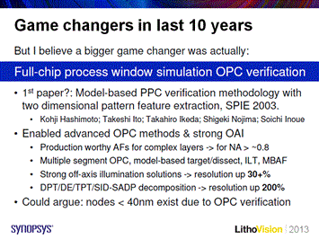
Figure 1A. As an example of a predicted future game changer that did not proceed as expected, Flagello showed an excerpt from a 1990 study by the Congressional Budget Office Study for Using R&D consortia (left image). Figure 1B. Lucas believes a key game changer of the past was full-chip process window simulation OPC verification.
Panelists Naoya Hayashi and Dr. Ralph Dammel had each spoken previously on their areas of expertise (described in a separate article in this edition). Hayashi discussed past game changers in next-generation lithography and cited mask challenges as a potential future change, and Dammel cited directed self-assembly (DSA) work and commented that the industry may move from a top-down to bottom-up style of lithographic patterning. Dr. Kevin Lucas reported that abandoning 157 nm in favor of 193 immersion lithography, which occurred 10 years ago, was a significant game changer, as its removal spurred the development of 193 nm immersion lithography, which enabled ~47% improvement in resolution. However, he believes a bigger game changer was actually full-chip process window simulation OPC verification (figure 1B). He described how this technology enabled advanced optical proximity correction (OPC) methods and strong off-axis illumination (OAI), with the OAI solutions driving resolution improvements by more than 30%. Moreover, it led to the decomposition techniques used in various double patterning schemes, boosting resolution by nearly 200%. He believes it could be argued that nodes below 40 nm exist due to OPC verification, and noted that verification methods continue to evolve. Looking to the future, Lucas said “To E(UV) or not to E(UV)? – that is the question,” and said that a key game changer in the next decade will be improving mask writing. He cited the need for increased cost-effectiveness of complex model-based AFs (MBAF), fine segment OPC (e.g., ILT), SADP for logic and memory periphery, triple patterning, and multiple cut-mask (complementary) lithography.
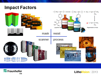
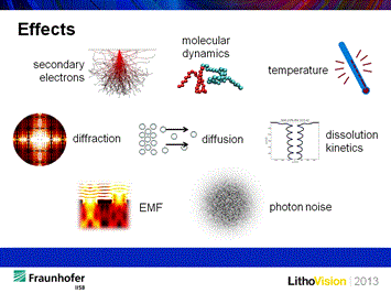
Dr. Andreas Erdmann spoke about the impact of lithographic modeling, showing a sample assessment of lithographic focus on electrical effects on a modeled device. He cited various game changers in lithography over the past years, such as the evolution of different resists and illumination schemes (figure 2A), and spoke of future modeling challenges including detailed resist effects like secondary electrons and molecular dynamics (figure 2B). Erdmann emphasized that different phenomena, like molecular dynamics, optics and electronics design, as well as resist chemistry, are inextricably linked in a complex network, and that lithographers will increasingly need to realize that they cannot separate their interdependencies.
-
Click image to enlarge.
Click image to enlarge.


Figure 2A. Erdmann cited various game changers in lithography over the past years, such as the evolution of different resists and illumination schemes (left image). Figure 2B. Erdmann spoke of future modeling challenges including detailed resist effects like secondary electrons and molecular dynamics.
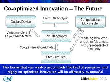
When considering how to extract the utmost performance from sizeable lithography investments, Sam Sivakumar believes source mask optimization (SMO) is the key game changer of the past. He noted that “pixel-level photon manipulation through SMO” has enabled full utilization of the potential of the scanner illumination system. He reminded the audience of edge placement error challenges, and warned that the overlay and critical dimension requirements may be scaling faster than the mechanical precision of the scanner stage. Therefore, Sivakumar believes co-optimized innovation will be essential in the future. Increased communication and cooperation between device design teams, lithographers, etch process engineers, and experts in computational lithography will be needed, and Sivakumar said that teams that can achieve this highly co-optimized innovation will be ultimately successful (figure 3A).
-
Click image to enlarge.
Click image to enlarge.
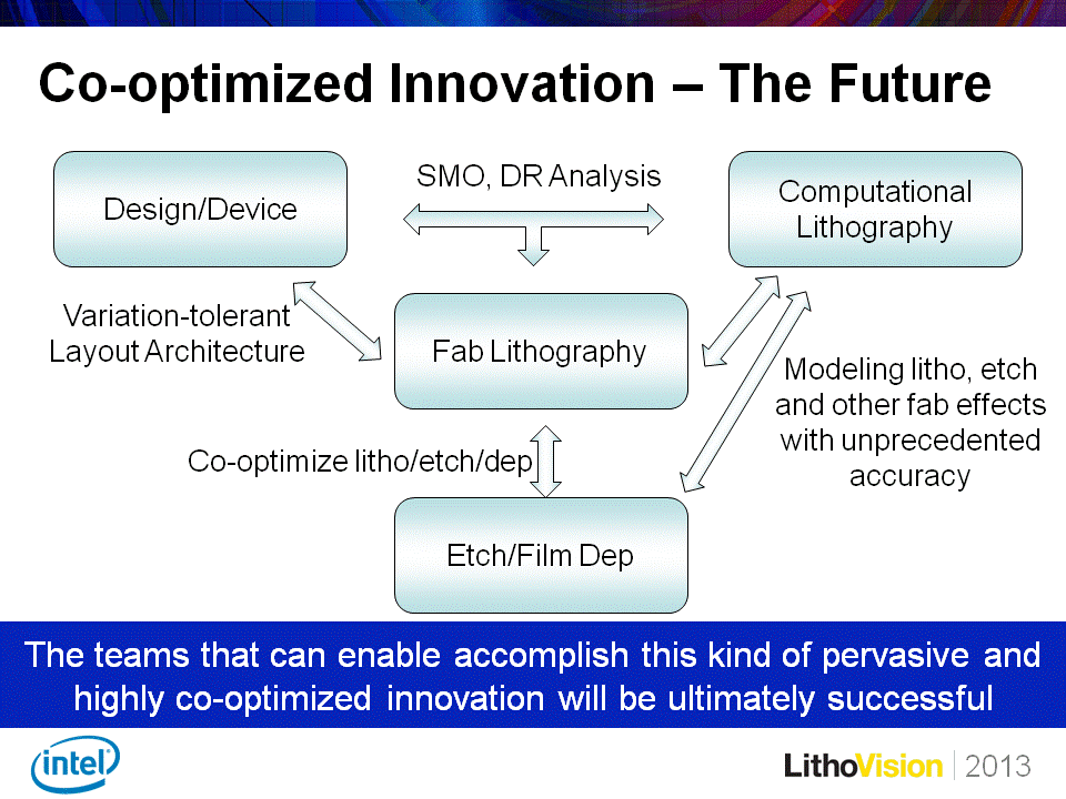

Figure 3A. Sivakumar believes co-optimized innovation will be essential in the future (left image). Figure 3B. Owa announced that the transition to 450 mm wafers will be a key game changer and that the future will likely be impacted by unpredictable NGL solutions.
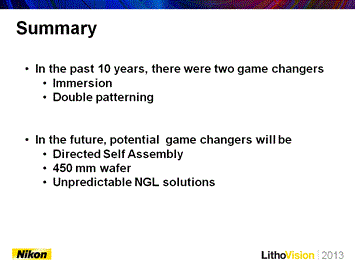
Dr. Soichi Owa ranked immersion lithography and double patterning as the key game changers of the last decade, as immersion made numerical apertures > 1.0 possible and double/multiple patterning continues to extend immersion capabilities. He agreed with Dammel’s assessment that DSA will play a vital role in the future. Owa announced that the transition to 450 mm wafers will be another key game changer. He likened the 300 mm to 450 mm wafer transition to that of the airline industry’s transition from jets transporting 150 passengers at a speed of 850 km/hour to the wide body Boeing 747, which could carry 350 to 500 passengers at 900 km/hour. He explained that 450 mm ArF scanners could deliver the necessary resolution and satisfy chip cost efficiency requirements. He also believes that the future will likely be impacted by unpredictable NGL solutions (figure 3B).
The panel discussion question and answer session opened with an audience member asking how far the industry had progressed in design for DSA. Panelists responded that the knowledge of basic material performance is lacking, and that basic modeling is “not there yet.” It was noted that data exists from experiments on basic processes. Flagello followed up by asking whether a compact model exists yet, and if not, whether it would be a game changer. The panel thought that it would be so, with Dammel commenting that current models, employing as they do only limited knowledge of molecular interaction potentials, are not good enough yet.
A related question from the audience asked about the resolution limit for DSA. Panelists were uncertain of the limit, but said that a different polymer would be needed to go below 10 nm. It was thought the limit may be around 4 to 5 nm, and the panel noted that even this will carry us through the next decade. Another audience member asked about e-beam direct-write lithography. The main issues cited by the panel included overlay and throughput, along with concerns about inherent noise due to electron-counting statistics. Throughput challenges are being investigated by chipmakers. It was also commented that it is difficult to develop resists for e-beam lithography since, as “an orphan technology,” the market remains small.
Finally the panelists were asked for their opinion of the biggest obstacle faced in the next ten years. Answers were:
- integration of DSA;
- the business model for next generation lithography (NGL) schemes, since so many players are small;
- cost structure for post-10 nm lithography;
- cost per mask;
- new design rules and integration;
- implementation of 450 mm wafers.
In summary, the diverse panel represented their respective segments of the industry extremely well, and provided a broad range of views on the key enabling technologies of the past decade. They also shared valuable insights regarding strategies and technologies that have significant potential to shape the industry in the future.