Immersion Extension and the Transition to 450 mm Highlighted at LithoVision
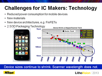
Speaking at the LithoVision symposium in February, Nikon General Manager Masato Hamatani discussed the criticality of ArF immersion extension due to ongoing delays in EUV infrastructure. His informative presentation on the “Industry Roadmap and Future Device Trends” addressed Nikon 193 nm scanner solutions as well as 450 mm platform extendibility. Hamatani’s presentation first highlighted the key applications driving the semiconductor industry through 2016 with notebook PCs, tablet PCs, and smartphones at 7.1%, 38.6%, and 21.4% unit growth respectively. These devices present a number of key technology challenges for IC makers including demand for reduced power consumption for mobile devices, new materials and device architectures (e.g. FinFETs), as well as 2.5/3D packaging; and although device sizes have continued to shrink, scanner wavelength has not (figure 1A). Furthermore, while semiconductor fabrication capital intensity continues upward for the advanced nodes, the prices of ICs are declining─making cost containment even more critical.
-
Click image to enlarge.

Click image to enlarge.
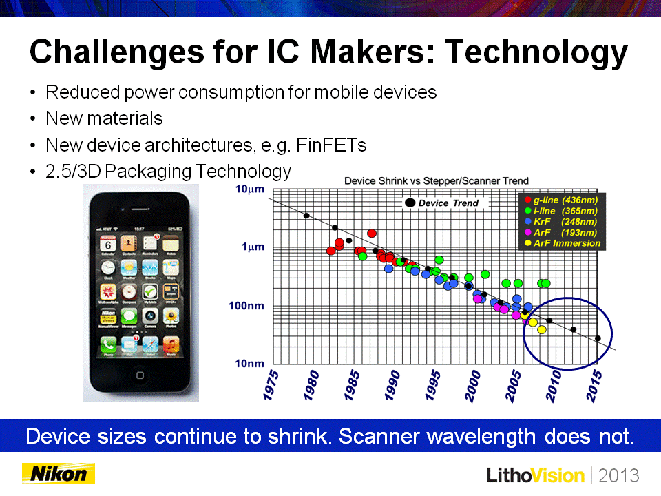
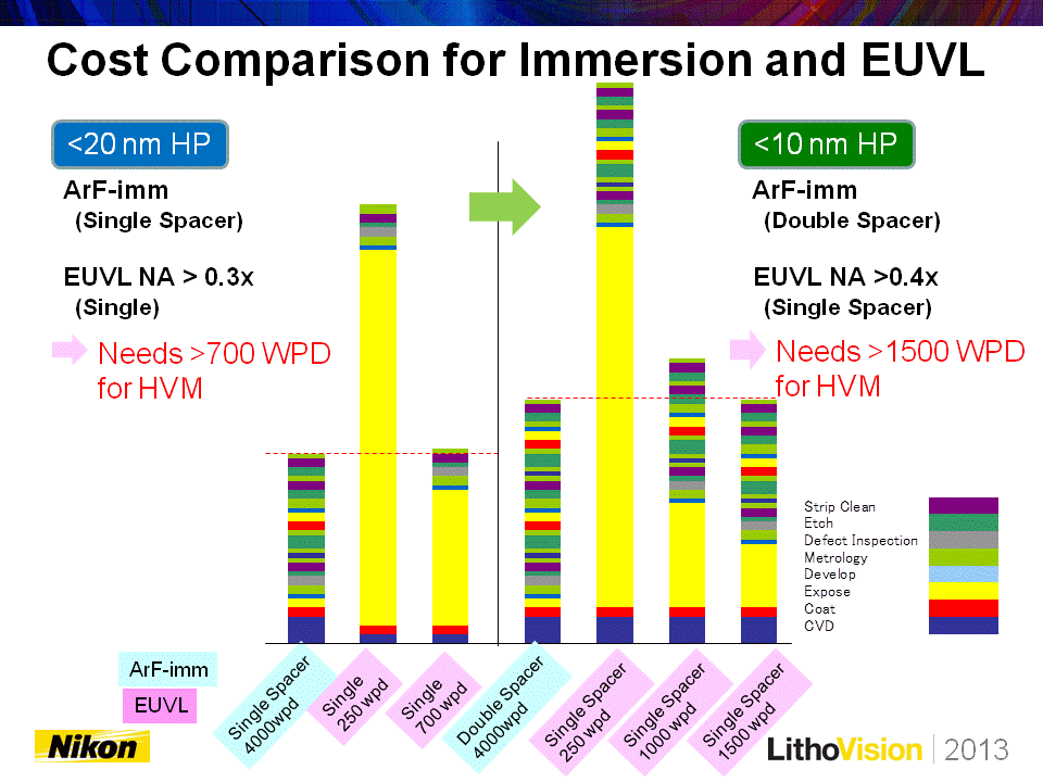
Figure 1A. Hamatani reported a number of technology challenges for IC makers (left image). Figure 1B. A cost comparison for immersion and EUVL shows that without significant advances in resist sensitivity and source power, it would be challenging for EUV to be economically viable even when compared to multiple patterning (MP).
At the EUV symposium in Brussels last fall, laser power, inspection infrastructure, and resist sensitivity were identified as the 2012 Key Focus Areas. Hamatani showed a cost comparison for immersion and EUVL, and he noted that, unless significant advances were made in both resist sensitivity and source power, it would be challenging for EUV to be economically viable even when compared to Multiple Patterning (MP) (figure 1B). Hamatani explained that Nikon continues to focus on ArF immersion extension, concentrating on providing constant improvement in performance, productivity, and application support software. Additionally, Nikon continues to work on compatibility with other next-generation lithography (NGL) solutions, like directed self-assembly.
To further improve 193 nm extension in the three areas above, Hamatani said that Nikon has released the NSR-S622D, delivering 3.5 nm mix-and-match overlay (MMO) with 200 wafers per hour (WPH) throughput for advanced multiple patterning applications. He also noted that the future S6XX immersion system will be available in 2015 with further MMO enhancements and increased productivity. There is a significant demand for critical layer, non-immersion ArF scanners as well, and Nikon continues to develop dry 193 nm technology. Hamatani announced that leading-edge throughput of the dry-ArF NSR-S320F scanner will be enhanced from 200 to 205 WPH and single machine overlay will be reduced from 3 nm to 2 nm later this year.
He explained that the key elements of ArF extension include improved imaging performance, enhanced overlay accuracy, and higher throughput, and described how the NSR-S622D immersion scanner addresses these areas. The latest evolution of the well-known Streamlign platform incorporates a new grid plate and encoder system, as well as minimized distortion to deliver enhanced overlay. This is combined with projection lens enhancements to reduce thermal aberrations, in addition to autofocus advancements and the Intelligent Illuminator Unit to deliver superior accuracy and performance for high volume manufacturing (figure 2A).
-
Click image to enlarge.
Click image to enlarge.
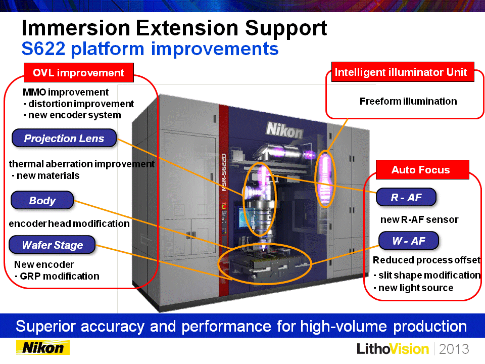
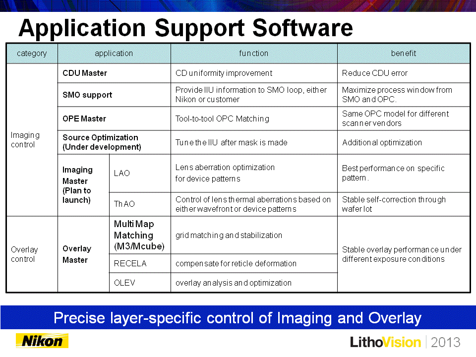
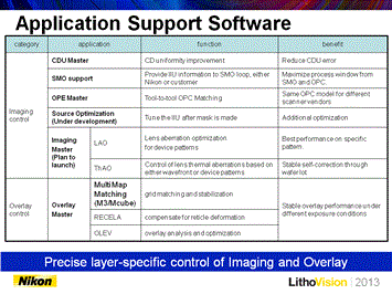
Figure 2A. The S622D scanner incorporates a number of design enhancements to enable immersion extension (left image). Figure 2B. Hamatani gave a brief introduction of the many Nikon software solutions that are available to aid immersion extension.
Hamatani reported that the S622D has demonstrated mix-and-match overlay stability between two S622D tools across 3 lots below 3.0 nm, and that autofocus uniformity including edge shots was only 11 nm. In addition, while the S622D is targeted for 4,200 wafers per day, further productivity improvements are being developed to satisfy manufacturing’s increasing requirements. Source and mask optimization (SMO) is vital in ArF extension and Hamatani reported that the S622D Intelligent Illuminator supports custom illumination and SMO. Precise layer-specific control of imaging and overlay are also essential for multiple patterning and Hamatani gave a brief introduction of the many Nikon software solutions that are available to aid immersion extension (figure 2B).
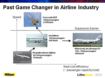
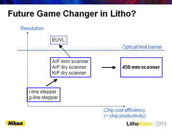
In the future, 450 mm wafers will bring greater economies of scale for semiconductor manufacturing, and Hamatani noted that they will reduce costs for property, plant, and equipment (PPE), in addition to manpower. The increased wafer size also slows the rise in per-unit-area process costs associated with technology evolution─an area where IC makers continue to struggle. In the LithoVision panel session, which focused on lithography “game changers” of the past and future, Nikon Fellow Dr. Soichi Owa, announced that the transition to 450 mm wafers will be a key game changer for lithography. He likened the transition from 300 mm to 450 mm wafers to that of the airline industry’s transition from jets transporting 150 passengers at a speed of 850 km/hour to the wide body Boeing 747, which could carry 350 to 500 passengers at 900 km/hour (figure 3A). He explained that 450 mm ArF scanners could deliver the necessary resolution and satisfy chip cost efficiency (figure 3B).
-
Click image to enlarge.
Click image to enlarge.

Figure 3A. Owa likened the transitioned from 300 mm to 450 mm wafers to that of the airline industry’s transition from jets to the wide body 747 (left image). Figure 3B. He explained that 450 mm ArF scanners could deliver the necessary resolution and satisfy chip cost efficiency.
The timing of the 450 mm transition will have a significant impact on the entire semiconductor industry. For it to be successful, collaboration between chipmakers, suppliers, and consortia is crucial. It is also necessary to leverage experience from the transition to, and standardization of 300 mm wafers. In order to satisfy the heightened manufacturing challenges presented at 450 mm while the industry is also transitioning to smaller feature sizes and utilizing multiple patterning techniques, lithography systems will require further enhancements to scanner overlay accuracy, throughput, and imaging performance. Hamatani explained that evolution of existing lithography technology will be a crucial success factor in this transition and reported that the proven Streamlign platform used on S621/S622D immersion and S320F scanners is effective in accommodating 450 mm wafers.
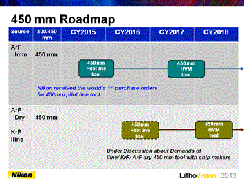
He also showed that Nikon 450 mm tool availability is well aligned with industry requirements and announced that Nikon has received the world’s first purchase orders for 450 mm ArF immersion pilot line tooling to ship in 2015, and will ship 450 mm high volume manufacturing tools in 2017 through joint development efforts with chipmakers (figure 4A). In the closing remarks at LithoVision, Toshikazu Umatate, Semiconductor Equipment Division General Manager and Company Vice President, added that with 450 mm manufacturing “the entire semiconductor industry can leap ahead,” and reaffirmed that the Nikon 450 mm program is steadily progressing.
-
Click image to enlarge.

Click image to enlarge.
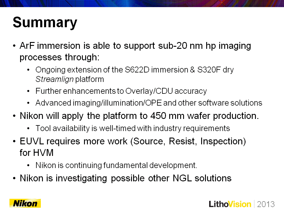
Figure 4A. Nikon 450 mm tool availability is well aligned with industry requirements with pilot line tooling to ship in 2015 and HVM equipment in 2017 (left image). Figure 4B. ArF immersion extension will continue and the proven Streamlign platform will be applied to 450 mm wafer production.
In Hamatani’s conclusion, he summarized that ArF immersion can support sub-20 nm half-pitch imaging requirements through extension of the Streamlign platform coupled with further enhancements to overlay and CD uniformity, as well as advanced imaging and software solutions to support computational lithography. He reminded the audience that Nikon will apply this platform to 450 mm wafer production, with tool availability well aligned with industry requirements. In addition, although the EUV infrastructure requires more work, Nikon continues fundamental EUV development in parallel with investigation of other possible next generation lithography solutions (figure 4B).