Dear Reader,
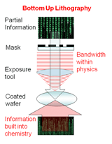
As you know, IC manufacturing technology continues to evolve and advance rapidly to meet next-generation requirements. The past year has been marked with tremendous enhancements to 193 nm scanners and new computational lithography solutions to extend ArF immersion capabilities. This is made even more exciting with 450 mm wafer capability coming firmly onto the roadmap and rapid progress in the very promising new game-changing technology of directed self-assembly.

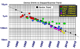
Many opportunities for innovation, as well as paradigm shifts in lithography technology and strategies were featured prominently at the 10th annual LithoVision technical symposium. More than 500 international representatives from across our industry attended the milestone event where industry experts from Nikon, GLOBALFOUNDRIES, Intel, AZ Electronic Materials, Dai Nippon Printing, Synopsys, and Fraunhofer IISB delivered insightful presentations discussing key lithography issues and solutions. The agenda showcased presentations on the Industry Roadmap and Future Device Trends, Enabling Production Beyond 20 nm, Mask and Materials Challenges for Next Generation Lithography, and more. An interactive panel discussion focused on key lithography events and innovations of the past 10 years, and discussed potential “game changers” for the future. In addition, the evening poster session featured informative contributions from a dozen partner companies. Highlights of several key LithoVision presentations are featured in this edition of the Nikon eReview, and full event materials are available to customers upon request.

In other news, Nikon has recently launched the NSR-S622D immersion scanner. The S622D is the latest evolution of the well-known Streamlign platform, and delivers unprecedented overlay performance and ultra-high productivity to satisfy the most aggressive sub-20 nm multiple patterning requirements.

Nikon values your input on how we can continue to improve our products, programs, and services, and we invite you to respond to the Nikon eReview (npicom@nikon.com) with your comments or suggestions.

Featured Article

DNP and AZ-EM Speakers Identify the Need for Lithography Paradigm Changes

At the recent LithoVision symposium, Dai Nippon Printing Fellow Naoya Hayashi and Dr. Ralph Dammel, Chief Technology Officer at AZ Electronic Materials, delivered presentations that highlighted paradigm shifts in mask and materials technology. Hayashi discussed the new requirements for mask making in an era of 193 nm extension and Dammel warned the audience that top-down patterning is running out of options.  


Read more

News

Immersion Extension and the Transition to 450 mm Highlighted at LithoVision

Speaking at the LithoVision symposium in February, Nikon General Manager Masato Hamatani discussed the criticality of ArF immersion extension due to ongoing delays in EUV infrastructure. His informative roadmap presentation addressed Nikon 193 nm solutions as well as 450 mm platform extendibility.


Read more

Intel and Nikon Litho Specialists Discuss Overlay Matching and Edge Placement Error for Production Beyond 20 nm

Litho Directors from Intel and Nikon Update on Enabling 32 nm Production and Beyond

Sam Sivakumar, Intel Corporation Fellow and Director of Lithography, reported at LithoVision that the biggest challenges to next-generation lithography are edge placement error and management of multiple exposure passes per layer. Nikon specialists also discussed how advancements in scanner mix-and-match overlay, focus, and CD control are enabling ArF immersion to support sub-20 nm half-pitch processes.


Read more

Technologists from GLOBALFOUNDRIES and Nikon Report on Computational Lithography Solutions in Manufacturing

Technologists from DNP and Nikon Discuss Computational Lithography Solutions

During the LithoVision symposium, Rolf Seltmann, GLOBALFOUNDRIES Fellow, explained the importance of vendor-to-vendor scanner matching and presented source mask optimization (SMO) results demonstrating marked improvements to process window and other metrics. Tomoyuki Matsuyama, Nikon Strategic Imaging Solutions Section Manager, delivered a complementary presentation describing Nikon computational lithography solutions for SMO, scanner matching, and post-mask optimization.


Read more

LithoVision Expert Panel: 10 Years of Litho – A Review and Look Ahead

NLithoVision Presentations Highlight EUV HVM Challenges and Nikon Advancements

Technology leaders from AZ-EM, Intel, DNP, Fraunhofer IISB, Synopsys and Nikon shared their opinions regarding key lithography events and innovations of the past 10 years, and discussed potential “game changers” for the future during the LithoVision panel moderated by Dr. Donis Flagello of Nikon Research.


Read more

Innovations and Enhancements

Enabling 193 nm Immersion Extension with Computational Lithography Solutions

Enabling ArF Extension with Overlay Enhancement Solutions

Extension of ArF or 193 nm immersion lithography is imperative for IC makers to maintain their roadmaps, with computational lithography a critical part of extending their capabilities. Extremely low k1 lithography processes require complex source shapes from source mask optimization as well as common OPC behavior from different scanner vendors. Additionally, these low k1 processes require stringent control of dose, focus, thermal aberrations, and CD uniformity. This necessitates comprehensive computational lithography solutions that can expand process windows and increase imaging robustness.


Read more

Nikon Happenings

LithoVision Reaches 10 Year Milestone

A record-tying audience joined Nikon for the 10th annual LithoVision technical symposium. More than 500 global representatives from throughout the semiconductor industry attended the milestone event where industry experts discussed key lithography issues and solutions.


Read more

Nikon Teams with Industry Partners to Support SEMI High Tech University

Nikon places great value on the opportunity to give back to our industry by providing support for next-generation engineers and leaders, and are pleased to continue our support for SEMI High Tech University.


Read more

Nikon Charitable Contributions Support Local and Global Organizations

Nikon Precision, through its Charitable Contributions Committee, is proud to support a number of charitable and non-profit organizations. Many contributions to national organizations and international relief efforts are ongoing annually, while other opportunities to support charitable endeavors are recommended by employees, or local Nikon offices.


Read more