LithoVision Reaches 10 Year Milestone
A record-tying audience joined Nikon for the 10th annual LithoVision technical symposium, held on February 24, 2013 in San Jose. More than 500 global representatives from throughout the semiconductor industry attended the milestone event where industry experts discussed key lithography issues and solutions. Respected presenters from Nikon, GLOBALFOUNDRIES, Intel, AZ Electronic Materials, Dai Nippon Printing, Synopsys, and Fraunhofer IISB offered their insights on the Industry Roadmap and Future Device Trends, Enabling Production Beyond 20 nm, Mask and Materials Challenges for Next Generation Lithography, and more.
-
Click image to enlarge.
-

Click image to enlarge.
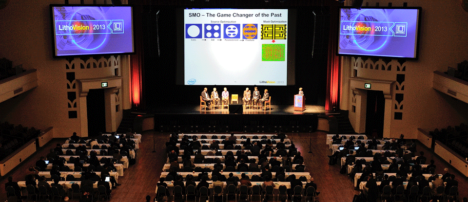
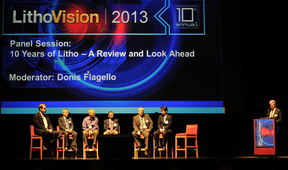
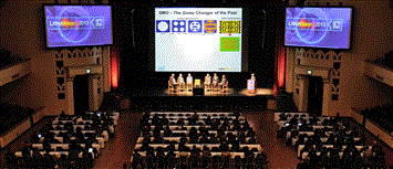
Figure 1A.More than 500 global representatives from throughout the semiconductor industry joined Nikon for the 10th annual LithoVision technical symposium on February 24, 2013. (left image). Figure 1B.An interactive panel session focused on key lithography events and innovations of the past 10 years, and potential “game changers” for the future.
New for LithoVision 2013 was an interactive panel discussion, moderated by Dr. Donis Flagello of Nikon Research Corporation of America, featuring a broad depth of technology leaders from across our industry. The panel focused on key lithography events and innovations of the past 10 years, and discussed potential “game changers” for the future. After the panelists shared their views, the session was opened for discussion and the audience was free to pose questions to the esteemed panelists. Attendee feedback cited the panel session as an excellent addition to the event, saying it provided valuable insight for the future of lithography from many key facets of the industry.
The 10th annual LithoVision showcased opportunities for innovation and paradigm shifts in lithography technology and strategies. Highlights of a number of the LithoVision presentations and the panel discussion are featured in this edition of the Nikon eReview, and full event materials are available to customers upon request.