QUALCOMM and Nikon Executives Report on the Industry Roadmap and Future Device Trends
Presenting the Nikon view of the Lithography Roadmap and Device Trends at the 2012 LithoVision symposium earlier this year, Masato Hamatani, General Manager of Stepper Development, began by identifying a number of challenges for IC makers. He reported that new chip architectures, 3D technology, film stack innovations, multiple exposures, and shorter exposure wavelengths are all tactics being explored to address design challenges. He further explained that customer technology requirements are driven by the need for transistor speed and enhanced yield, while cost challenges necessitate increased scanner productivity and reliability to maximize wafers per day as well as tool reuse capabilities to enable usage at multiple generation nodes.
Hamatani then described the scanner technology challenges and ways to meet customer requirements. He explained that ArF immersion extension is the primary solution, and noted it is able to support sub-20 nm half pitch (hp) processes. However, he cautioned that this requires overlay improvements to support multiple exposures, enhanced illumination flexibility to enable complex pattern fidelity and source mask optimization (SMO), increased throughput at reduced costs, and support for 450 mm wafers.
Hamatani reported that the “next” potential technology, EUVL, necessitates higher NA optics to enable future technology nodes, compatibility with high output sources (when they become available), in addition to consideration of wavelength changes and/or other advancements. As a supplementary solution, he noted that scanner manufacturers must study new techniques such as directed self-assembly (DSA) with immersion and/or EUVL. These novel solutions may work with or without EUVL to enable the litho roadmap.
-
Click image to enlarge.
Click image to enlarge.
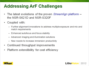
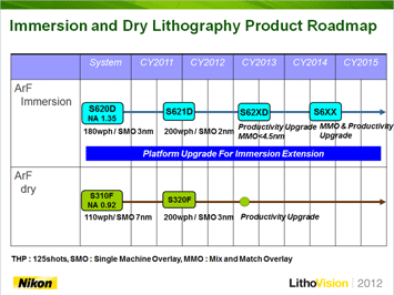
Figure 1. Hamatani explained how Nikon is addressing ArF requirements with the NSR-S621D immersion and NSR-S320F dry ArF scanners (left image). He also shared the immersion and dry lithography product roadmap highlighting ArF scanner extension.
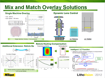
Hamatani later revealed how Nikon is addressing the key ArF customer requirements with the latest generation NSR-S621D immersion and NSR-S320F dry ArF scanners, which are based on the proven Streamlign platform employed on the NSR-S620D. He also shared the immersion and dry lithography product roadmap, highlighting ArF scanner extension. In addition, Hamatani identified a number of mix-and-match overlay solutions including Dynamic Lens Control, Reticle Bending, and Reticle Heating Compensation that were developed to support double patterning (DP), as well as autofocus improvements made to respond to the challenges of chip architecture and IC maker film stack innovations. He also provided an overview of imaging and illumination solutions that are available to support SMO, and reported ongoing progress with ArF scanner productivity.
In addition, Hamatani announced that S620D reticle stage and wafer stage/encoders can be upgraded to the S621-type to enhance overlay accuracy, and that the S620D nozzles can also be changed to reduce defects and boost productivity. He explained that such solutions enable tool reuse and aid in cost management.
-
Click image to enlarge.
Click image to enlarge.

Figure 2. Hamatani discussed mix-and-match overlay solutions developed to support DP (left image). He commented that ArF immersion is able to support sub-20 nm hp imaging processes and Nikon continues to develop tools to satisfy industry requirements.
Hamatani also reported that the transition to 450 mm is one of the most important cost reduction methods for chip makers and noted that Streamlign technology is suitable for a 450 mm platform to support this critical process cost reduction. Hamatani rounded out his presentation with a brief discussion of EUVL technology. He commented that a numerical aperture >0.4 will be required for EUVL to ensure that the k1 factor, a measure of the difficulty of imaging, is kept at a reasonable level for the 16 nm hp – 11 nm hp nodes. Otherwise, techniques such as Double Patterning would be required for EUVL. He also commented that efforts investigating the possibility of a 6.7 nm source are in the research phase for potential use beyond the 10 nm hp node. In his conclusion, Hamatani announced that Nikon is developing optics for higher NA or shorter wavelength EUVL to be available when the EUVL infrastructure is ready for high volume manufacturing.
In a complementary presentation, Dr. Geoffrey Yeap, VP of Technology and Foundry Engineering of QUALCOMM provided insight to the Roadmap Requirements and Device Trends from the fabless perspective. Yeap began his talk with discussion of the “Connected Mobile Life” of this decade and the convergence of the internet—anytime, anywhere, for anyone. He reported a 34% year over year increase in U.S. consumers accessing the web via mobile devices and highlighted that the overall demand for data continues to grow at a phenomenal rate.
-
Click image to enlarge.
Click image to enlarge.

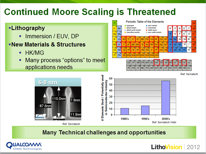
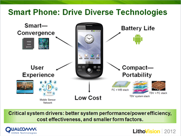
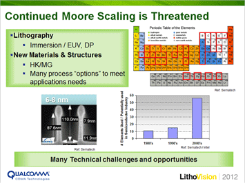
Figure 3. As an example, Yeap showed the ways that smart phones drive diverse technologies (left image). Yeap cautioned that continuation of Moore’s scaling is being threatened by a number of technical and economic challenges.
Yeap proceeded to describe how semiconductor innovation is a critical enabler for this growth, and as an example showed the ways that smart phones drive diverse technologies by requiring better system performance/power efficiency, cost effectiveness, and smaller form factors. Yeap cautioned however, that continuation of Moore’s scaling is being threatened by a number of technical and economic challenges. He reported that improvements to lithography and new materials as well as process and defect optimization are essential for continued scaling economics, and stressed that cost effectiveness is vital to success.
-
Click image to enlarge.

Click image to enlarge.
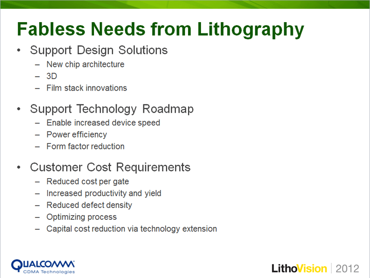
Figure 4. Yeap highlighted there are many cost challenges and identified improvement areas that are essential for continued scaling economics (left image). He also identified various fabless lithography requirements.
Yeap transitioned to the topic of the fabless lithography requirements, highlighting the importance of providing support for design solutions and the technology roadmap, as well as customer cost requirements. He conveyed the criticality of adding value through lithography extensions and noted the following needs:
| - | For 20 nm: enable 80 nm or below pitch single patterning copper metal/via for chip P&R -> smaller die size and lower cost |
- |
For 20 nm: enable cost-effective and tight local interconnect module for dense standard cell library, |
| - | For 14 nm: enable sub-64 nm metallization pitch double patterning |
Finally, Yeap described the importance of having an integrated fabless model and how collaboration across the entire eco-system (including foundry, packaging, EDA, IP, research, customers, etc.) is required for optimized product innovation and execution.
Yeap summarized his informed presentation by reminding the audience that innovative technology scaling and “More than Moore” solutions are required to meet the challenges of low cost, performance/power efficiency and smaller form factors. He noted that multi-design of architecture, circuit and design, silicon and packaging/test are required for the development of superior products that meet customer requirements, and he stressed that collaboration across the entire eco-system is essential.