NIST, CEA-Leti, and Nikon Leaders Address Extending Lithography with DSA
In an informative presentation at the LithoVision conference, Dr. Gregg Gallatin, a physicist at the Center for Nanoscale Science and Technology at the National Institute of Standards and Technology (NIST), educated the audience on the potential for directed self-assembly (DSA) of block copolymers (BCP) for advanced lithography. Gallatin began by explaining that block copolymers are composed of two different types of string-like molecules tied together at one end that repel each other and so automatically self-assemble into nm-scale periodic features when laid on an appropriate substrate. This is relevant to lithographers since the use of BCPs may circumvent challenging issues with resists used in EUV lithography. The resist phenomenon known as the “triangle of death” means that it is very challenging to simultaneously meet requirements for resolution < 20 nm half-pitch (hp), line edge roughness (LER) < 1.0 nm 3σ and sensitivity < 10 mJ/cm2. He referred to the 2011 ITRS Roadmap, which identified the potential values of DSA using BCP as enabling higher-density features than lithography and reduced LER. Gallatin also highlighted that 7 nm features and 2.2 nm LER have been achieved using DSA, although not simultaneously.
-

Click image to enlarge.
Click image to enlarge.
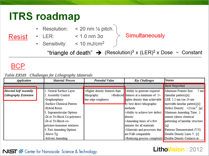
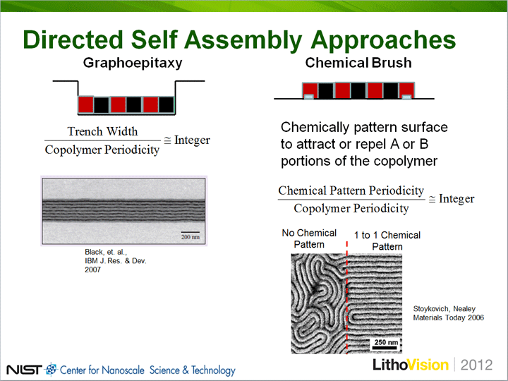
Figure 1. Gallatin referred to the 2011 ITRS roadmap highlighting DSA for litho extension (left image). He noted that the BCP assembly must be properly directed to achieve the desired features.
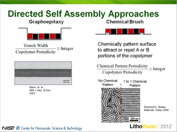
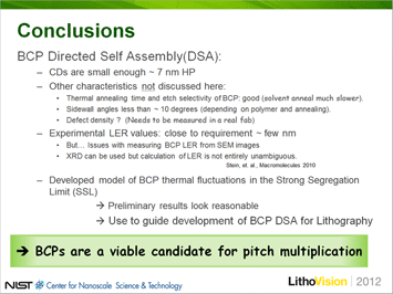
The BCP assembly must be properly directed in order to achieve the desired features; Gallatin cited Graphoepitaxy and a Chemical Brush process as possible approaches for this. The chemical-brush process uses a chemically patterned surface to attract or repel specific segments of the copolymer whereas in Graphoepitaxy the BCP is physically bound by features between which the BCP arranges itself once processed. Modeling of lamellar BCP patterns shows that thermal fluctuations cause line-edge roughness and to get LER values below 2 nm may require inordinately high values of the Flory-Huggins parameter, which is a measure of the strength of the repulsion between the two types of molecules making up the copolymer. Gallatin reported that experimental results have shown that LER values obtained using BCP appear close to the requirements (~ few nm), but warned that SEM imaging can yield inconsistent results. He stated that other imaging methods can be used, but in all cases care is needed with the analysis of the measurement. In Gallatin’s summary he concluded that BCPs are a viable candidate for pitch multiplication.
-

Click image to enlarge.
Click image to enlarge.
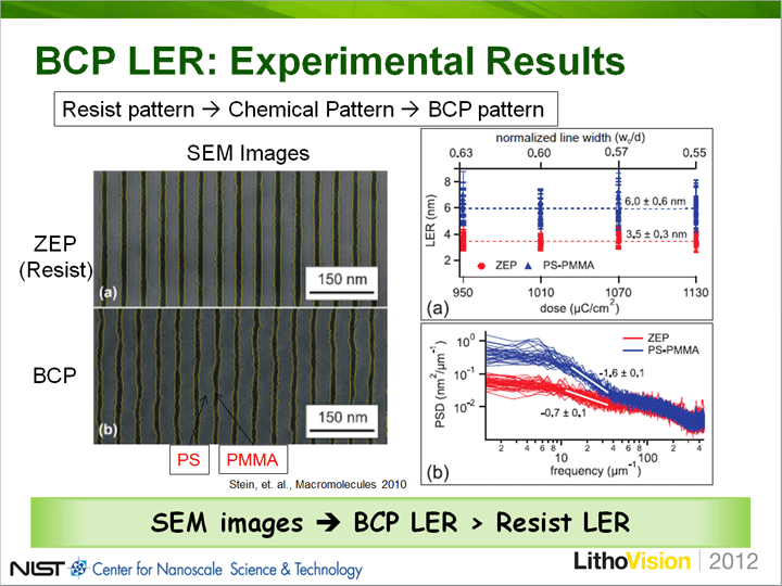
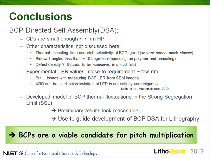
Figure 2. Gallatin cautioned about issues with measuring the BCP line edge roughness using SEM images (left image). He concluded that BCPs are a viable candidate for pitch multiplication.
Nikon and SPIE Fellow Dr. Soichi Owa also addressed the possibilities of DSA. He reported that using optical-based multiple patterning it is possible to reach ~10 nm hp, and stated that line cutting lithography is a potential solution for production of 1x nm hp devices. He explained how DSA could then be used to reduce the associated process complexity.
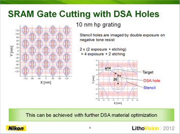
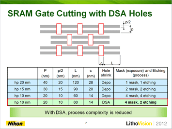
Owa began by showing potential uses of DSA for line/space and hole cutting applications, and then delved into discussion of an SRAM gate cutting example application. He explained that while a hole shrink deposition process would require a total of 4 masks and 4 etch steps at the 10 nm hp, if DSA was instead used for the hole shrink, then the etch steps could be cut in half. Thus, with further DSA materials optimization, the process complexity would be reduced. He concluded by noting that NSR-S620D and S621D immersion scanners are being used for double and multi-patterning in manufacturing, and announced that Nikon is focusing on 193 nm immersion technology to support these next-generation solutions.
-
Click image to enlarge.
Click image to enlarge.
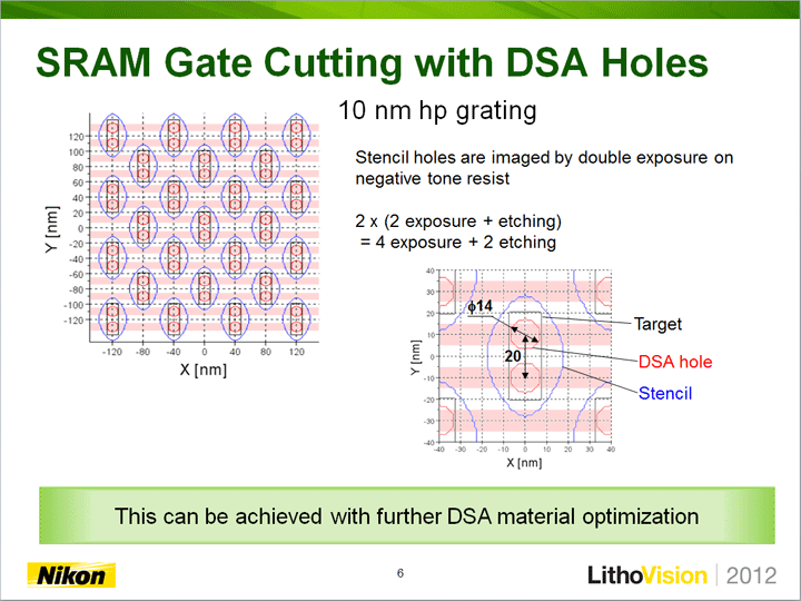

Figure 3. Owa showed an SRAM gate cutting application (left image) using DSA. He explained that with DSA materials optimization, the process complexity would be reduced.
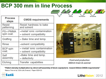
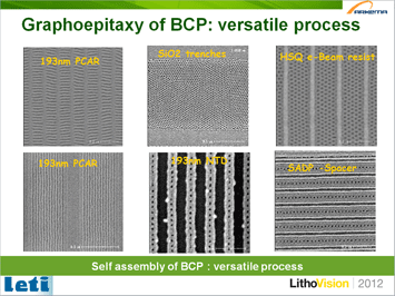
Doctors Serge Tedesco and Raluca Tiron of LETI then provided further details on DSA using BCPs at the event. Tedesco’s presentation reinforced the resolution, LER, process, and cost benefits of BCPs to the audience. However, he also identified a number of CMOS lithography constraints, which included control of domain orientations (1D-2D), alignment, integration capabilities, low defectivity, and respect of design rules. Tiron’s poster highlighted the LETI Graphoepitaxy process and she reported that BCP self-assembly is compatible with 193 nm lithography and can be processed using existing lithography equipment. The LETI presentations also provided insight to the BCP 300 mm in-line process and showed the process steps and CMOS requirements.They reported that the copolymer etching process is fully compatible with CMOS requirements and stressed the versatility of the BCP Graphoepitaxy self-assembly process. It was further noted that directed self-assembly using BCP is compatible with a wide variety of materials. In addition to DSA having shown the capability to address resolution and pitch for contact level printing, Tiron stated that increasing the BCP film thickness also decreased the number of resist-polymer interaction defects and commented this may be a potential defectivity reduction strategy.
-
Click image to enlarge.
Click image to enlarge.


Figure 4. The LETI presentations provided insight to the BCP 300 mm in-line process (left image). The versatility of the BCP Graphoepitaxy self-assembly process was highlighted.
Together, these presentations from across the industry provided LithoVision attendees with an excellent view of the potential for directed self-assembly and how it can be used to extend ArF immersion lithography.