Experts from Tokyo Electron and Mentor Graphics Report On
Optical Litho Extensions
Speaking recently at the LithoVision technical symposium, Hidetami Yaegashi, Senior Manager at Tokyo Electron Limited, conveyed the need to extend 193 immersion (193i) optical lithography for continued lithographic scaling. With data from the NSR-S610C immersion scanner (NA = 1.30) and the TEL Lithius Pro-i+, he began by showing the audience a successful self aligned double patterning (SADP) process used to create 20 nm half-pitch (hp) lines from 40 nm hp lines. He then explained that this technique can be extended to more complicated features by combining the SADP process with cutting lithography. In this "spacer and cut" process, SADP is followed with a second litho step, hole shrink, and cutting to finish with 20 nm hp 2D structures. A second possible process technique, which instead used a BARC and SiARC etch with a hardmask etch, was also shown to be quite effective. It was also highlighted that there has been great progress in SADP applications, with downward scaling and advancements in 2D pattern formation occurring simultaneously.
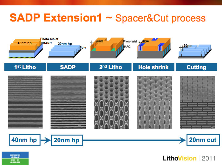
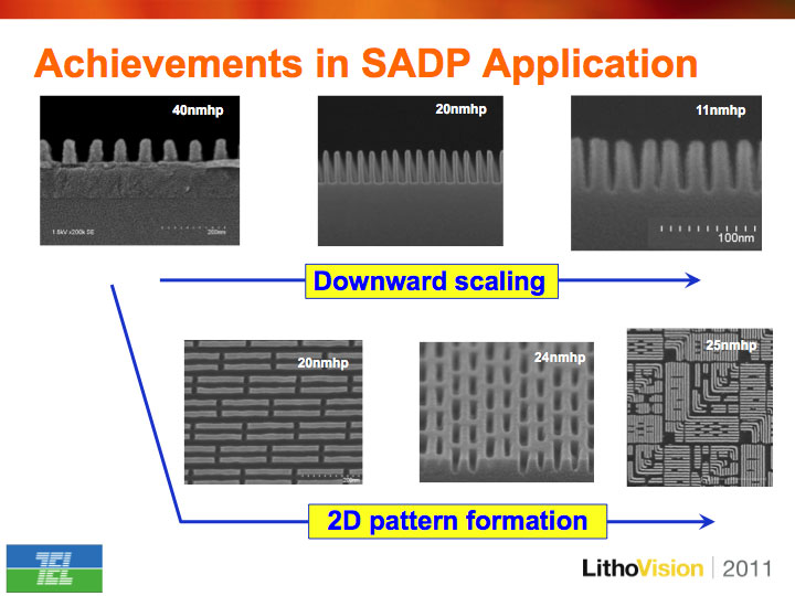
Figure 1. SADP processes have been extended to yield 20 nm hp 2D structures (left image). Great progress in SADP applications was reported, with downward scaling and advancements in 2D pattern formation occurring simultaneously.
Yaegashi then discussed continued scaling using pitch quadrupling, and showed multiple techniques that were used to successfully yield 11/12 nm lines, but cautioned about the differences in costs of the methods used to create them. The importance of refining the pitch quadrupling schemes to be cost aware was also highlighted. Looking further at cost implications, cost of ownership (CoO) estimates for 20 nm SRAM gates and 22 nm short trenches comparing various ArFi and EUV exposure options were shown. Yaegashi explained that spacer-based double patterning costs are lower than initially expected, with much of the necessary deposition equipment being significantly less expensive than next generation lithography tools. He also highlighted potential CoO advantages when compared to EUVL, such as in the case of 1D layouts using optimized SADP processes. He further commented that throughput sensitivities are critical for CoO, and noted that EUVL throughput as high as 150 wafers per hour (WPH) may be required to gain any cost advantages.
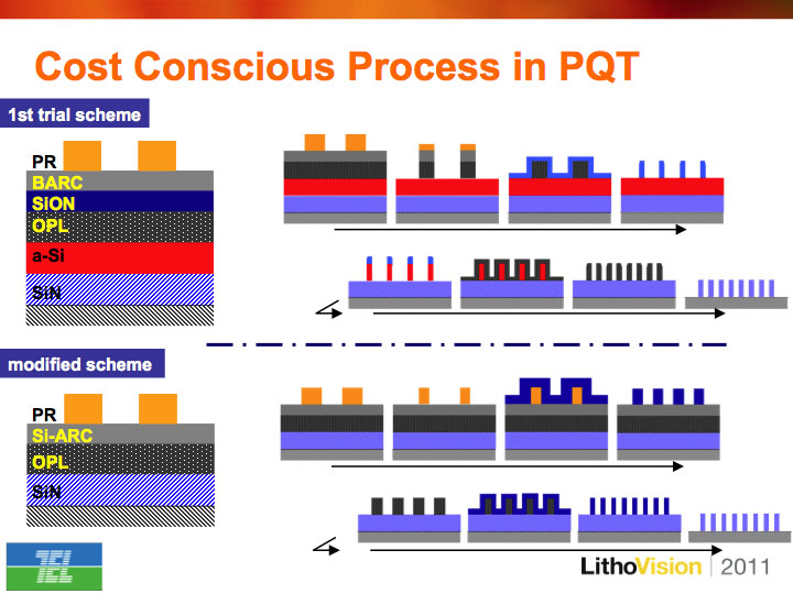
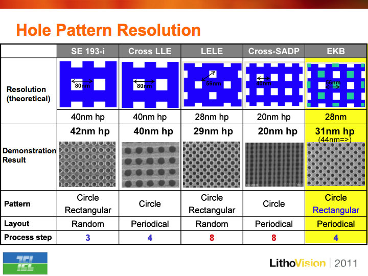
Figure 2. The importance of refining the pitch quadrupling schemes to be cost aware was highlighted (left image). Contact-hole patterning from various techniques was also shown.
Contact-hole patterning that showed data from various techniques including a Cross-SADP technique with 8 process steps (producing 20 nm contact holes) and single-exposure techniques using various intermediate process and etch steps, was next discussed. CoO analyses for contact holes showed potential advantages of various multiple patterning solutions when compared to EUVL at 60 WPH. It was noted that while a double patterning scheme presents greater process complexity compared to EUV, the additional investment (tool price) associated with the deposit tools required for the DP process were only 5% of the EUVL tool price.
Yaegashi concluded his informative presentation by reiterating that 193i optical litho must be extended for continued scaling, with SADP being one potential technique for fine pattern fabrication beyond 193i resolution capabilities. In addition, he noted that this method has wide extendibility for 2D pattern formation on single orientation layouts in future complementary litho applications.
Speaking next at LithoVision, Dr. Gandharv Bhatara, Mentor Graphics Product Marketing Manager, reported on the "Computational Lithography Challenges for Extending Optical Immersion Lithography." He opened his presentation by explaining how scaling drives computational requirements for optical proximity correction (OPC). He noted that the average number of computational operations is approximately 4× higher and the normalized computational load has increased by nearly 15× when comparing 65 nm to 22/20 nm processes. Bhatara also discussed the types of verifications required to enable the semiconductor roadmap, saying that while at 65 nm only multi-dimension checks, litho checks, and pitch checks were needed, for 22 nm and beyond, on-grid checks, pattern match, and double patterning checks will be necessary. The multitude of additional techniques that will be required to enable low k1 ArF immersion lithography extension to 22 nm, which include double patterning (DP), source and mask optimization, model assisted SRAFs, and resolution enhancement technique (RET) optimization were also highlighted.
Bhatara next explained that double patterning enforces design restrictions, and noted that resolving conflicts is critical in its design enablement. For instance, OPC approaches must satisfy overlay and CD uniformity criteria, and inaccurate recombination of DP split masks (where a layout had been split across two masks) can lead to significant overlay issues. He proceeded to discuss the limitations in current Sequential Double Patterning OPC flows, and how they can lead to inefficient solutions. It was noted that when using a sequential method, since the first mask exposure has no information on the second mask results or problems, the second mask must then "fix" any overlay problems encountered during the first mask OPC. He said that a better proposed solution is a Concurrent DP OPC flow where concurrent OPC correction of both masks allows for information sharing between the two corrections during the OPC process, and commented that this method resolves any mask rule check (MRC) issues resulting from double patterning decomposition.
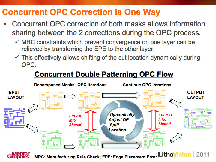
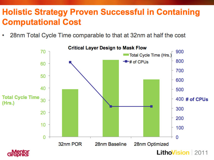
Figure 3. It was reported that a Concurrent DP OPC flow allows for information sharing between the two corrections during the OPC process (left image). A holistic strategy has enabled 28 nm total cycle time comparable to that of 32 nm–at half the cost.
Bhatara then turned to discussion of source-mask optimization, concentrating on the mask aspect, and noted that while this clearly enables significant process window (PW) benefits, it brings with it challenges with respect to increased shot counts, mask inspection and MRC, and runtime. He reported that a variety of strategies exist to obtain an acceptable shot count, including concurrent optimization for shot count as well as downstream shot count reduction with innovative fracturing. He then commented that when it comes to managing inspection and MRC, the standards for inspection and applying manufacturability criteria are changing and therefore require close collaboration with mask makers.
It was subsequently stressed that the increased complexity of modern mask designs is causing a software problem and making full-chip mask optimization computationally unfeasible. Bhatara explained that a holistic solution that integrates CPU utilization and scalability, core software performance, tapeout flow optimization, optimization for hardware, and reduced memory consumption is needed to manage this. He then showed that such a strategy has proven quite successful in containing computational cost, with 28 nm total cycle time being comparable to that of 32 nm, but at half the cost.
Concluding his insightful presentation on extending optical lithography, Bhatara summarized that extending ArF lithography requires innovative and sophisticated techniques such as double patterning and source-mask optimization. He stressed that DP places unique requirements on OPC approaches and design enablement, and necessitates a bridge between design and mask synthesis. He also reported that advanced mask optimization is becoming a reality with issues such as shot count and mask inspection challenges being resolved, and highlighted that a holistic strategy can be effective in containing runtime costs.