Litho Directors from Intel and Nikon Update on Enabling 32 nm
Production and Beyond
At the recent LithoVision 2011 technical symposium, Yuichi Shibazaki, S620 Technical Director and General Manager of Next Generation Development, reported on the latest NSR-S620D performance data and provided information on further evolution of the Streamlign Platform system for enhancing performance in mass production and extending ArF immersion (ArFi). Shibazaki began by announcing that the 200 wafer per hour (WPH) target has been achieved and showed S620D results having processed more than 5100 wafers in a 24 hour period, using a single exposure stage system. He reported that this great achievement is made possible by the Stream Alignment system, which enables simultaneous wafer alignment and autofocus mapping.
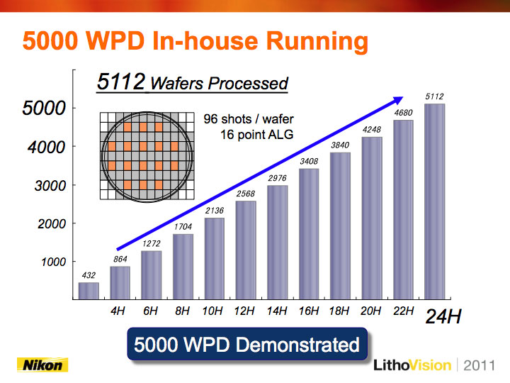
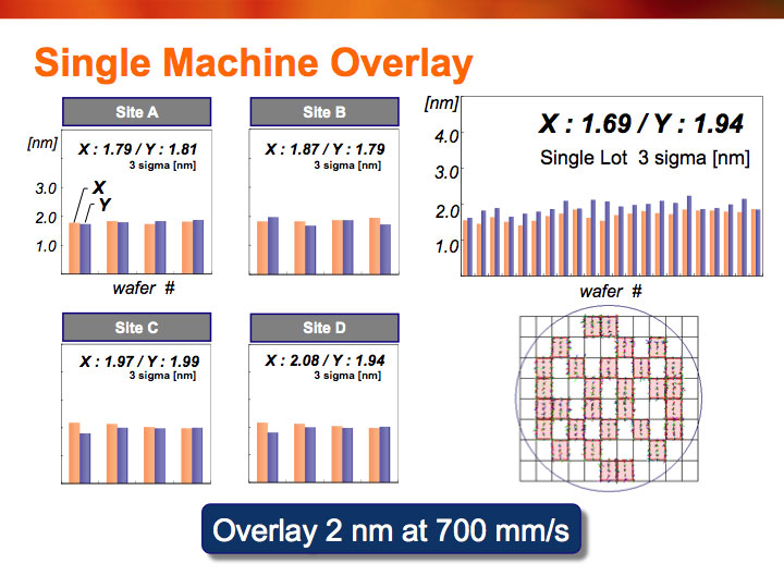
Figure 1. The S620D has processed >5100 wafers in a 24 hour period, using a single exposure stage system (left image). Stream Alignment also provides enhanced tool accuracy with 2 nm overlay confirmed.
Shibazaki explained that Stream Alignment, in addition to maximizing throughput, also increases alignment accuracy with Five-Eye FIA, a system using five alignment microscopes. He shared overlay accuracy results obtained from 4 different sites – all at 700mm/sec scan speed -- and announced that S620D 2 nm overlay capabilities have been confirmed. Shibazaki showed 5 day overlay stability data below 3 nm, as well as mix-and-match overlay with the S610C < 6 nm. Finally he showed excellent focus control data, made possible by Straight Line Autofocus, which covers the entire wafer surface, and sophisticated Z control. Full-wafer focus uniformity less than 12.7 nm (including edge shots) was obtained at multiple sites.
Shibazaki then discussed Nikon solutions to further enhance scanner performance for mass production and to extend ArFi capabilities. He noted that overlay requirements become increasingly challenging with double patterning (DP), and commented that while Nikon already provides a variety of functions to correct for grid and shot shape errors, a new function has been developed that corrects shot shape by changing lens magnification during scanning. This dynamic lens control adds trapezoid (k9), hourglass and barrel (k17) shot shape corrections, thereby providing an additional knob for enhanced tool adjustment and matching. Noting also the criticality of CD uniformity for DP, Shibazaki proceeded to explain the newly developed Adaptive Reticle Chuck that is able to correct for image plane curvature induced by heating, the pellicle, residual projection lens error, or reticle manufacturing. He explained that by bending the reticle using the force of its chuck, these curvatures can be corrected free of side effects.
Shibazaki wrapped up his detailed tool update by noting that, after achieving 200 WPH and 2 nm overlay, S620D performance is now being optimized for manufacturing at customers’ sites, and he reiterated that Nikon has developed comprehensive solutions to further extend ArFi capabilities.
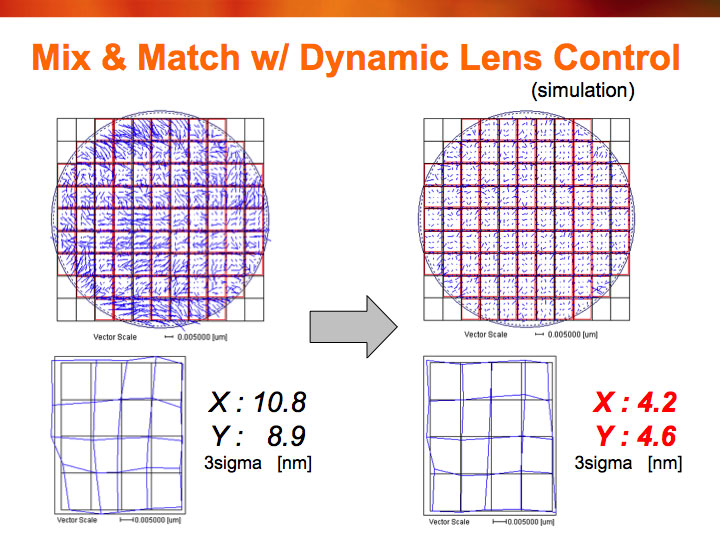
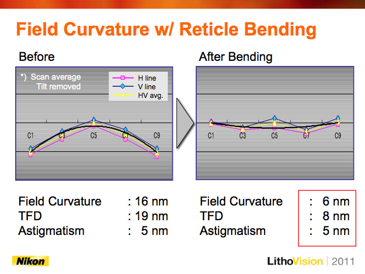
Figure 2. Dynamic lens control provides enhanced tool matching with added shot shape correction capabilities (left image). The Adaptive Reticle Chuck reduces field curvature, independent of side effects.
Speaking next at the event, Sam Sivakumar, Intel Corporation Fellow and Director of Lithography, reported on "Enabling the Future – From 32 nm Production to 14/10 nm Development." Sivakumar began by giving the audience the status of Intel’s 32 nm ArF-immersion process technology, commenting that it has ramped successfully and achieved yield parity with previous dry lithography strategies. In addition, he noted that the NSR-S620 is progressing well towards the high volume manufacturing (HVM) ramp, with mix-match overlay showing HVM-quality results.
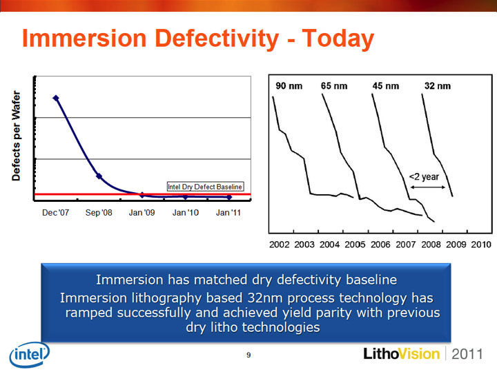
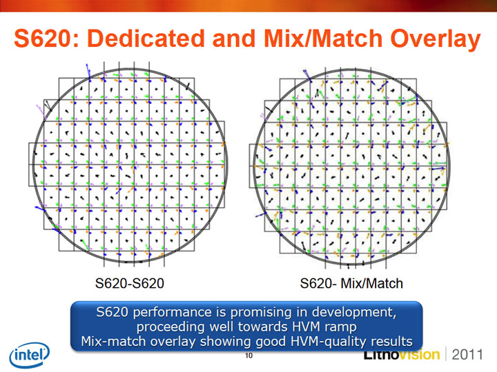
Figure 3. Sivakumar reported 32 nm immersion process technology has ramped successfully and achieved yield parity with previous dry litho (left image). He noted that the NSR-S620 is progressing well towards the HVM ramp, with mix-match overlay showing HVM-quality results.
Sivakumar then commented that 22 nm development is also on track, with the high volume ramp scheduled for the second half of 2011 using immersion lithography. Looking next at the 14 nm node, with HVM targeted for 2013, Sivakumar compared ArF pitch division with EUVL. He reported that while EUVL has advantages with regard to using single exposure and having simpler design rules, Sivakumar indicated that EUVL technology readiness timing put it outside the scope of 14 nm.
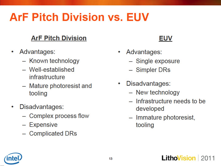
Figure 4. Sivakumar compared the advantages and disadvantages for ArFi pitch division versus EUVL (left image) for 14 nm HVM. Sivakumar stressed that 10 nm DR definition will start before production EUV tools arrive.
Sivakumar looked next at the 10 nm node HVM in 2015, referring to Yan Borodovsky’s 2010 LithoVision presentation, which discussed the potential for using ArFi with complementary lithography, and highlighted the possibility for 10 nm using 5 ArFi masks, but questioned the cost and design rule (DR) restrictions. He commented on the EUV resist/reticle status as a candidate for that node and commented that while resist resolution is looking reasonable, further work is still required on line edge roughness and sensitivity. He also highlighted that reticle blank defectivity is still in the critical path.
Sivakumar stressed that 10 nm design-rule definition will start before production EUV tools arrive, and cautioned the audience that the design rules for ArF vs. EUV paths are very different, highlighting that close process/design interaction and design flexibility will be vital to success. He concluded his insightful presentation by noting that while EUV is a lead option, ArFi is technically capable of meeting the patterning requirements for the 10 nm node.