Nikon Fellow Inducted as 2010 SPIE Fellow
We are very pleased to announce that Soichi Owa, Nikon Fellow and Technology Development Section Manager, was named a 2010 SPIE Fellow in recognition of his achievements in optical microlithography—in particular immersion lithography, as well as solid state lasers. SPIE is the international society for optics and photonics founded in 1955 to advance light-based technologies. SPIE Fellows are Members of distinction who have made significant scientific and technical contributions in the multidisciplinary fields of optics, photonics, and imaging. They are honored for their technical achievement, for their service to the general optics community, and to SPIE in particular.
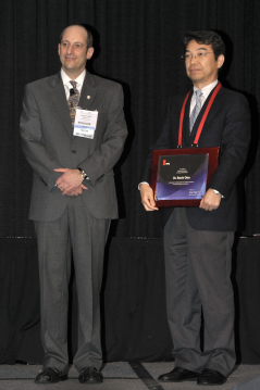
Soichi Owa with 2010 SPIE Advanced Lithography Symposium Chair Christopher Progler.