Intel Sr. Fellow Recommends Complementary Solutions for ArF Extension
Presenting his view on ArF Lithography Extension for Critical Layer Patterning at the LithoVision symposium held earlier this year, Yan Borodovsky, Intel Corporation Sr. Fellow and Director of Advanced Lithography, began his presentation by showing that improved SRAM fidelity/uniformity has been delivered for each technology generation, while still maintaining a 2x bitcell area scale. He then highlighted that with the start of 32 nm production in 2009, ArF lithography had been utilized in high volume manufacturing (HVM) for 8 years, and proceeded to show that this existing technology has many more years of extendibility.
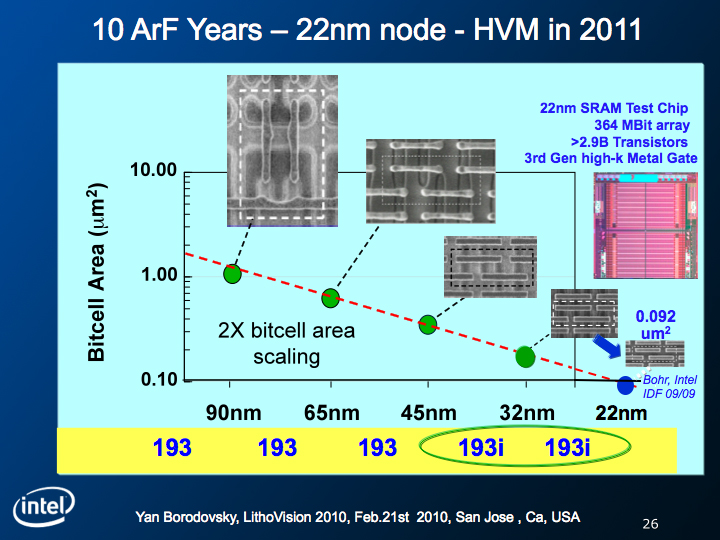
Figure 1. Improved SRAM fidelity/uniformity has been delivered for each technology generation, while also maintaining a 2x bitcell area scale.
Borodovsky reported that 193 nm immersion (193i) lithography will be carried forward to the 22 nm node in 2011. Looking further, he reported that since 193i lithography using pitch division (PD) is currently the only solution available to support patterning for 15 nm logic design rule (DR) definition, then it will be the default approach for 15 nm node logic HVM in 2013. He then explained that multiple PD methods are currently being investigated to determine the optimum solution for density, wafer cost, and design productivity co-optimization.
Borodovsky identified a number of benefits for continuing to the 6
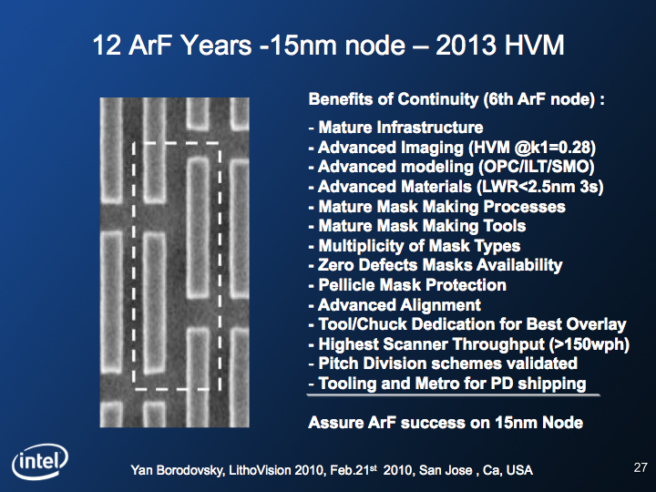
Figure 2. Borodovsky reported that 193i using PD will be the default approach for 15 nm node logic HVM in 2013.
Looking next at the 11 nm node, Borodovsky reported that "193i with pitch division can and will be extended as a viable option for Intel HVM patterning in 2015." However, he cautioned that this may require several masks per layer for logic layouts, and proceeded to highlight potential gaps in cost, cycle time, and process complexity associated with this approach. Therefore, Borodovsky instead proposed a Complementary Patterning approach for 2015 and beyond. He showed that with ArF immersion-only patterning, a total of 5 masks and 5 exposures would be required for the simple layout pattern scaled down to expected 2015 HVM logic node dimensions. In contrast, Complementary Patterning, incorporating techniques such as EUV lithography or electron beam direct write (EBDW), would not exceed 2 masks/2 exposures per critical layer—while at the same time taking advantage of mature 193i patterning technology.
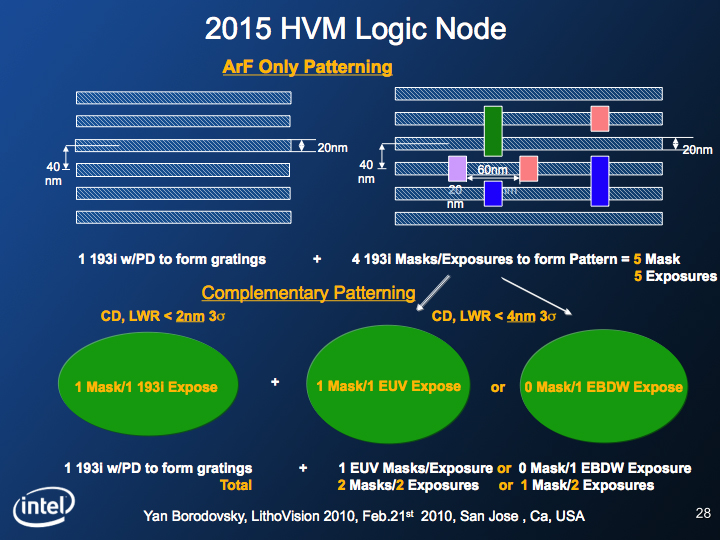
Figure 3. Borodovsky showed that with ArF-only patterning, a total of 5 masks and 5 exposures would be required for the 2015 HVM logic node. In contrast, Complementary Patterning, incorporating techniques such as EUVL or EBDW, would not exceed 2 masks/2 exposures per critical layer.
He explained that learning for HVM using 193i+EUV Complementary could begin using existing 0.25 numerical aperture (NA) systems, with aggressive illumination EUV for 11 nm node design rule (DR) development for DR definition completion following, and noted that an NA > 0.3 would allow use of less restrictive illumination in development and HVM. In addition, Borodovsky highlighted that the complementary use of EUVL will relax mask defect and mask inspection requirements for EUV insertion in high volume manufacturing, and that new 193-based imaging systems may have adequate sensitivity for mask blank inspection for this application. This complementary approach would enable the earliest EUV insertion in high volume manufacturing. He reported that EBDW could also be used instead of EUV for the complementary solution to break the continuity of the grating made using 193i with pitch division. In addition to again maintaining the benefits of mature 193i on the critical layer, this solution has lower mask costs (no mask required for grating cutting and vias), and the escalating cost of the mask-making infrastructure is avoided.
Borodovsky summarized his informative presentation by concluding that 193 immersion will be extended to support the established area density and patterning fidelity trends for use in high volume manufacturing in 2011 and 2013. Then, complementing 193i with solutions such as EUVL or EBDW will enable 193i patterning extension to 2015 logic manufacturing with minimized process complexity and cost. In addition, this complementary approach will enable next generation lithography (NGL) insertion into high volume manufacturing at the most favorable conditions, thereby preventing further NGL manufacturing introduction slips and reducing insertion risk for customers.