SPIE Plenary by Nikon President Addresses "The Future of Optical Lithography"
Kazuo Ushida, President of Nikon Precision, had the honor of delivering a plenary presentation on "The Future of Optical Lithography" at SPIE Advanced Lithography 2010. As the opening speaker for the technical conferences, Ushida began his presentation with an overview of the market trends. He showed that the semiconductor industry is indeed maturing, with only single digit revenue growth likely in the future. He also reported that although the next few years look encouraging for wafer fab equipment revenue, he highlighted that conditions are not expected to return to previous record levels.
Ushida then transitioned to discussion of the Future of Optical Lithography, framing his presentation around issues for Yesterday, Tomorrow, and Today. Looking first at "The Next Generation, Yesterday", Ushida shared cost of ownership (CoO) data estimates from 1999 for a variety of lithography technologies. In spite of the investigated techniques having comparable CoOs, he noted that none of them were actually implemented, as DUV extension was instead determined to be the simplest path to continue on the industry roadmap.
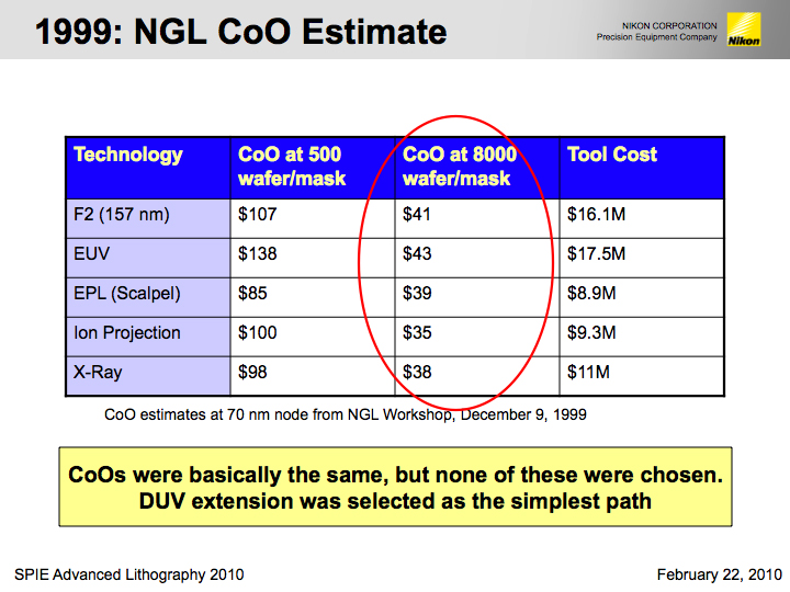
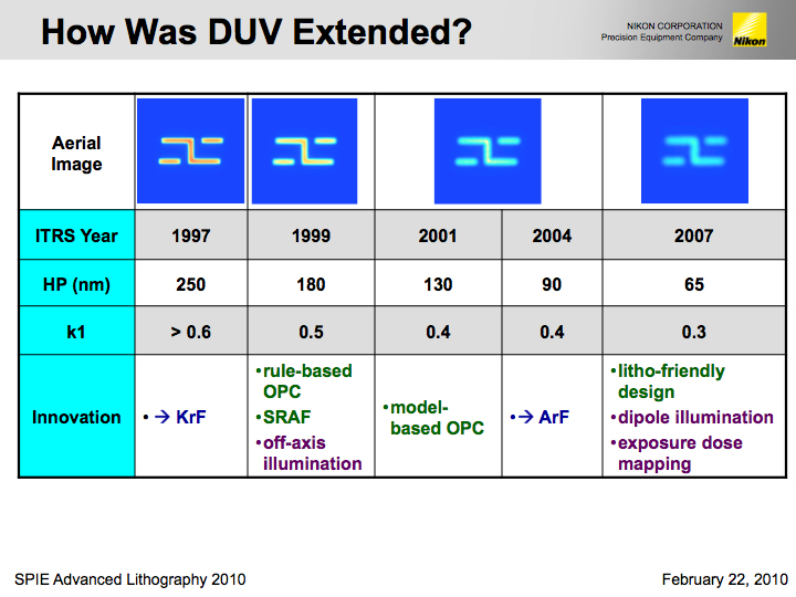
Figure 1. Ushida reported that in spite of comparable next generation lithography (NGL) CoO estimates, DUV extension was chosen as the simplest path in 1999 (left image). He highlighted the various methods used to extend DUV capabilities over time.
Ushida explained that rather than transition to new and unfamiliar technologies, DUV capabilities continued to be extended by reducing the k1 factor using innovations such as increasingly sophisticated optical proximity correction (OPC), off-axis illumination, dipole illumination strategies, and exposure dose mapping. Ushida then highlighted that in parallel, the industry also adopted argon fluoride (ArF) light sources, while scanner lens designs have been pushed to deliver numerical apertures (NA) once thought impossible.
When the maximum NA using dry ArF lithography was finally achieved, and k1 was at levels not practical for manufacturing, the industry determined that the next logical step was to again extend DUV through the introduction of immersion technology. Immersion adoption moved very quickly, and Ushida shared an overview of the aggressive Nikon immersion tool history. It began with initial Engineering Evaluation Tools (EET) launched in 2004, and progressed to the leading-edge NSR-S620D for double patterning (DP) applications, which began shipping in Q4'2009.
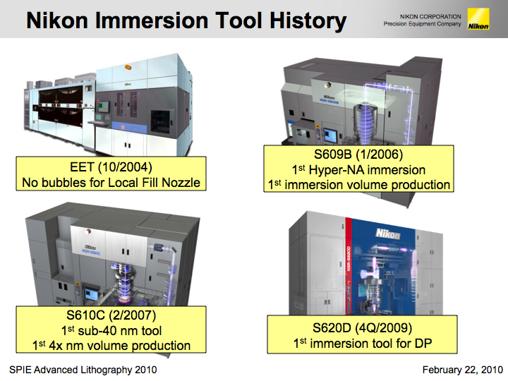
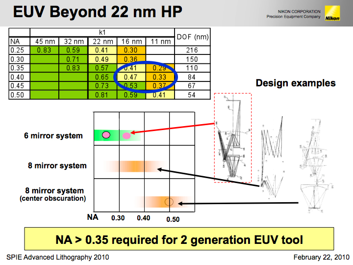
Figure 2. Ushida shared an overview of the aggressive Nikon immersion tool history (left image). He noted that a EUV system NA > 0.35 will be required to enable multi-generational tool capabilities.
Ushida then focused on "The Next Generation, Tomorrow", and identified a variety of the on-going issues with EUV lithography (EUVL). He commented on the significant time and cost still required for mask infrastructure development as well as the subsequent time required for defectivity learning, and reported that EUV will be too late for many IC makers' 22 nm half-pitch (hp) roadmaps. Ushida also noted that in order to enable multigenerational tool capability and justify tool cost, a EUV system NA > 0.35 will actually be required, and concluded that these factors will delay EUV introduction until the 16 nm half pitch.
Moving next to discussion of "The Next Generation, Today", Ushida presented several alternatives to EUVL. He identified ways to extend single patterning such as source mask optimization (SMO) and customized illumination. He also identified solutions to enable the 32 nm half pitch and beyond including spacer and pitch splitting DP, as well as line cutting lithography. Ushida showed that the 20 nm hp has already been achieved using the previous generation NSR-S610C immersion scanner. In spite of pitch splitting overlay challenges, the S610C has also demonstrated 20 nm half-pitch capabilities using litho-etch-litho-etch DP. Ushida reported that various double patterning solutions, as well as line cutting lithography with SMO, will be used to extend ArF immersion to the 22 nm hp and beyond. Ushida then identified various ways that DP cost of ownership will be reduced to support ArF immersion extendibility. This included the employment of multilayer masks (both DP patterns are on the same mask), which can reduce small lot costs by ~50%, as well as multigenerational platform capabilities to enable tool reuse for the 22 nm hp, which can cut large lot costs by more than 20%.
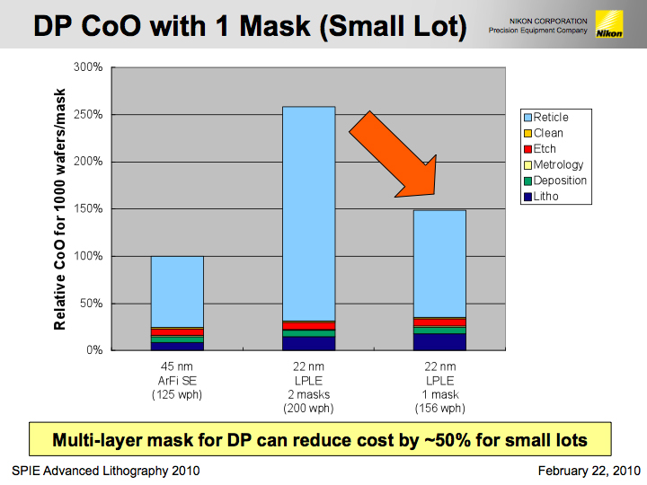
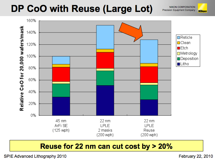
Figure 3. Ushida explained how the use of multi-layer masks can reduce small lot costs dramatically (left image), while multi-generational platform capabilities will cut large lot costs.
Ushida concluded his plenary presentation by showing how the Nikon NSR-S620D immersion scanner is enabling the future of ArF immersion lithography. He reported that the S620D maximizes yield through 2 nm overlay accuracy using Bird's Eye Control and enhanced CD control with dose/focus tuning capabilities; delivers affordable lithography by targeting 200 wafers per hour throughput using Stream Alignment; and ensures the fastest time to IC manufacturing profitability with the Modular